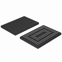
SSTUB32865ET/G,518 NXP Semiconductors, SSTUB32865ET/G,518 Datasheet - Page 26

SSTUB32865ET/G,518
Manufacturer Part Number
SSTUB32865ET/G,518
Description
IC REG BUFFER 28BIT 160TFBGA
Manufacturer
NXP Semiconductors
Datasheet
1.SSTUB32865ETG518.pdf
(28 pages)
Specifications of SSTUB32865ET/G,518
Logic Type
1:2 Registered Buffer with Parity
Supply Voltage
1.7 V ~ 2 V
Number Of Bits
28
Operating Temperature
0°C ~ 70°C
Mounting Type
Surface Mount
Package / Case
160-TFBGA
Logic Family
SSTU
Logical Function
Reg Bfr W/ParityTst
Number Of Elements
1
Number Of Inputs
28
Number Of Outputs
56
High Level Output Current
-8mA
Low Level Output Current
8mA
Propagation Delay Time
3ns
Operating Supply Voltage (typ)
1.8V
Operating Supply Voltage (max)
2V
Operating Supply Voltage (min)
1.7V
Clock-edge Trigger Type
Posit/Negat-Edge
Polarity
Non-Inverting
Technology
CMOS
Frequency (max)
450(Min)MHz
Mounting
Surface Mount
Pin Count
160
Operating Temp Range
0C to 70C
Operating Temperature Classification
Commercial
Lead Free Status / RoHS Status
Lead free / RoHS Compliant
Other names
568-3542-2
935281691518
SSTUB32865ET/G-T
935281691518
SSTUB32865ET/G-T
Available stocks
Company
Part Number
Manufacturer
Quantity
Price
Company:
Part Number:
SSTUB32865ET/G,518
Manufacturer:
NXP Semiconductors
Quantity:
10 000
NXP Semiconductors
14. Abbreviations
15. Revision history
Table 17.
SSTUB32865_3
Product data sheet
Document ID
SSTUB32865_3
Modifications:
SSTUB32865_2
SSTUB32865_1
Revision history
Release date
20070327
20060922
20060807
•
•
•
For further information on temperature profiles, refer to Application Note AN10365
“Surface mount reflow soldering description” .
Table 16.
Acronym
CMOS
DDR2
DIMM
DRAM
LVCMOS
RDIMM
SSTL
The format of this data sheet has been redesigned to comply with the new identity guidelines of
NXP Semiconductors.
Legal texts have been adapted to the new company name where appropriate.
Table 10
Fig 23. Temperature profiles for large and small components
MSL: Moisture Sensitivity Level
temperature
“Characteristics”, I
Abbreviations
Data sheet status
Product data sheet
Product data sheet
Product data sheet
Description
Complementary Metal Oxide Semiconductor
Double Data Rate 2
Dual In-line Memory Module
Dynamic Random Access Memory
Low Voltage Complementary Metal Oxide Semiconductor
Registered Dual In-line Memory Module
Stub Series Terminated Logic
Rev. 03 — 27 March 2007
= minimum soldering temperature
DD
(max) for static standby current changed from “100 A” to “2 mA”
maximum peak temperature
minimum peak temperature
= MSL limit, damage level
1.8 V DDR2-800 registered buffer with parity
Change notice
-
-
-
SSTUB32865
temperature
Supersedes
SSTUB32865_2
SSTUB32865_1
-
peak
© NXP B.V. 2007. All rights reserved.
001aac844
time
26 of 28


