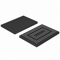
SSTUB32865ET/G,518 NXP Semiconductors, SSTUB32865ET/G,518 Datasheet - Page 18

SSTUB32865ET/G,518
Manufacturer Part Number
SSTUB32865ET/G,518
Description
IC REG BUFFER 28BIT 160TFBGA
Manufacturer
NXP Semiconductors
Datasheet
1.SSTUB32865ETG518.pdf
(28 pages)
Specifications of SSTUB32865ET/G,518
Logic Type
1:2 Registered Buffer with Parity
Supply Voltage
1.7 V ~ 2 V
Number Of Bits
28
Operating Temperature
0°C ~ 70°C
Mounting Type
Surface Mount
Package / Case
160-TFBGA
Logic Family
SSTU
Logical Function
Reg Bfr W/ParityTst
Number Of Elements
1
Number Of Inputs
28
Number Of Outputs
56
High Level Output Current
-8mA
Low Level Output Current
8mA
Propagation Delay Time
3ns
Operating Supply Voltage (typ)
1.8V
Operating Supply Voltage (max)
2V
Operating Supply Voltage (min)
1.7V
Clock-edge Trigger Type
Posit/Negat-Edge
Polarity
Non-Inverting
Technology
CMOS
Frequency (max)
450(Min)MHz
Mounting
Surface Mount
Pin Count
160
Operating Temp Range
0C to 70C
Operating Temperature Classification
Commercial
Lead Free Status / RoHS Status
Lead free / RoHS Compliant
Other names
568-3542-2
935281691518
SSTUB32865ET/G-T
935281691518
SSTUB32865ET/G-T
Available stocks
Company
Part Number
Manufacturer
Quantity
Price
Company:
Part Number:
SSTUB32865ET/G,518
Manufacturer:
NXP Semiconductors
Quantity:
10 000
NXP Semiconductors
11. Test information
SSTUB32865_3
Product data sheet
11.1 Test circuit
All input pulses are supplied by generators having the following characteristics:
Pulse Repetition Rate (PRR)
unless otherwise specified.
The outputs are measured one at a time with one transition per measurement.
Fig 8. Load circuit
Fig 9. Voltage and current waveforms; inputs active and inactive times
Fig 10. Voltage waveforms; pulse duration
(1) C
(1) I
CK inputs
V
V
V
DD
ID
IH
IL
L
includes probe and jig capacitance.
= V
tested with clock and data inputs held at V
= 600 mV.
= V
ref
ref
+ 250 mV (AC voltage levels) for differential inputs. V
R L = 100
test point
test point
250 mV (AC voltage levels) for differential inputs. V
RESET
input
LVCMOS
50
Rev. 03 — 27 March 2007
I
DD
(1)
10 MHz; Z
0.5V
t
INACT
DD
V
10 %
ICR
CK
CK
DUT
0
1.8 V DDR2-800 registered buffer with parity
= 50 ; input slew rate = 1 V/ns
OUT
t
W
DD
or GND, and I
delay = 350 ps
Z o = 50
0.5V
V
ICR
t
IL
IH
ACT
O
DD
= GND for LVCMOS inputs.
= 0 mA.
= V
C L = 30 pF (1)
SSTUB32865
002aaa373
V
0 V
DD
DD
V
002aaa372
ID
for LVCMOS inputs.
90 %
V
V
IH
IL
© NXP B.V. 2007. All rights reserved.
V
DD
R L = 1000
R L = 1000
002aaa371
20 %,
18 of 28


