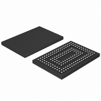
SSTUB32865ET/G,518 NXP Semiconductors, SSTUB32865ET/G,518 Datasheet - Page 6

SSTUB32865ET/G,518
Manufacturer Part Number
SSTUB32865ET/G,518
Description
IC REG BUFFER 28BIT 160TFBGA
Manufacturer
NXP Semiconductors
Datasheet
1.SSTUB32865ETG518.pdf
(28 pages)
Specifications of SSTUB32865ET/G,518
Logic Type
1:2 Registered Buffer with Parity
Supply Voltage
1.7 V ~ 2 V
Number Of Bits
28
Operating Temperature
0°C ~ 70°C
Mounting Type
Surface Mount
Package / Case
160-TFBGA
Logic Family
SSTU
Logical Function
Reg Bfr W/ParityTst
Number Of Elements
1
Number Of Inputs
28
Number Of Outputs
56
High Level Output Current
-8mA
Low Level Output Current
8mA
Propagation Delay Time
3ns
Operating Supply Voltage (typ)
1.8V
Operating Supply Voltage (max)
2V
Operating Supply Voltage (min)
1.7V
Clock-edge Trigger Type
Posit/Negat-Edge
Polarity
Non-Inverting
Technology
CMOS
Frequency (max)
450(Min)MHz
Mounting
Surface Mount
Pin Count
160
Operating Temp Range
0C to 70C
Operating Temperature Classification
Commercial
Lead Free Status / RoHS Status
Lead free / RoHS Compliant
Other names
568-3542-2
935281691518
SSTUB32865ET/G-T
935281691518
SSTUB32865ET/G-T
Available stocks
Company
Part Number
Manufacturer
Quantity
Price
Company:
Part Number:
SSTUB32865ET/G,518
Manufacturer:
NXP Semiconductors
Quantity:
10 000
NXP Semiconductors
Table 3.
SSTUB32865_3
Product data sheet
Symbol
Ungated inputs
DCKE0, DCKE1
DODT0, DODT1
Chip Select gated inputs
D0 to D21
Chip Select inputs
DCS0, DCS1,
DCS2, DCS3
Re-driven outputs
Q0A to Q21A
Q0B to Q21B
QCS0A, QDS1A,
QCS0B, QCS1B
QCKE0A, QCKE1A,
QCKE0B, QCKE1B
QODT0A, QODT1A,
QODT0B, QODT1B
Parity input
PARIN
Parity error
PTYERR
Pin description
[1]
6.2 Pin description
Pin
U1, U2
T2, T1
M1, B1, B2, C1, C2, D2, D1,
E1, E2, F2, M2, F1, G2, R1,
L2, H2, N2, N1, G1, P1, R2,
P2
J2, K2, H4, K4
V11, F12, G12, V6, V9, H12,
L12, V8, V12, N12, M12,
P12, V7, V10, T12, R12,
E12, A12, A10, A9, D12, A8
U11, F11, G11, U6, U9,
H11, L11, U8, U12, N11,
M11, P11, U7, U10, T11,
R11, E11, A11, B10, B9,
D11, B8
J12, K12, J11, K11
A7, A6, B7, B6
B12, C12, B11, C11
A3
U4
Rev. 03 — 27 March 2007
Type
SSTL_18
SSTL_18
SSTL_18
SSTL_18
SSTL_18
open-drain When LOW, this output indicates that a parity error was
Description
DRAM function pins not associated with Chip Select.
DRAM inputs, re-driven only when Chip Select is LOW.
DRAM Chip Select signals. These pins initiate DRAM
address/command decodes, and as such at least one will
be LOW when a valid address/command is present. The
register can be programmed to re-drive all D-inputs only
(CSGATEEN = HIGH) when at least one Chip Select
input is LOW. DCS2 and DCS3 are not re-driven and can
be left open-circuit to default HIGH by means of its
internal pull-up resistors.
Outputs of the register, valid after the specified clock
count and immediately following a rising edge of the
clock.
Parity input for the D0 to D21 inputs. Arrives one clock
cycle after the corresponding data input.
identified associated with the address and/or command
inputs. PTYERR will be active for two clock cycles, and
delayed by an additional clock cycle for compatibility with
final parity out timing on the industry-standard DDR2
register with parity (in JEDEC definition).
1.8 V DDR2-800 registered buffer with parity
SSTUB32865
© NXP B.V. 2007. All rights reserved.
6 of 28


