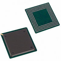
DS33R11+ Maxim Integrated Products, DS33R11+ Datasheet - Page 7

DS33R11+
Manufacturer Part Number
DS33R11+
Description
IC ETH TXRX T1/E1/J1 256-BGA
Manufacturer
Maxim Integrated Products
Type
Transceiverr
Datasheet
1.DS33R11.pdf
(344 pages)
Specifications of DS33R11+
Protocol
T1/E1/J1
Voltage - Supply
1.8V, 3.3V
Mounting Type
Surface Mount
Package / Case
256-BGA
Lead Free Status / RoHS Status
Lead free / RoHS Compliant
Number Of Drivers/receivers
-
- Current page: 7 of 344
- Download datasheet (12Mb)
DS33R11 Ethernet Mapper with Integrated T1/E1/J1 Transceiver
Figure 12-19. Transmit-Side 2.048MHz Boundary Timing (Elastic Store Enabled)................................................ 307
Figure 12-20. Receive-Side Timing ......................................................................................................................... 308
Figure 12-21. Receive-Side Boundary Timing (with Elastic Store Disabled) .......................................................... 308
Figure 12-22. Receive-Side Boundary Timing, RSYSCLK = 1.544MHz (E-Store Enabled)................................... 309
Figure 12-23. Receive-Side Boundary Timing, RSYSCLK = 2.048MHz (E-Store Enabled)................................... 309
Figure 12-24. G.802 Timing, E1 Mode Only............................................................................................................ 310
Figure 12-25. Transmit-Side Timing ........................................................................................................................ 310
Figure 12-26. Transmit-Side Boundary Timing (Elastic Store Disabled)................................................................. 311
Figure 12-27. Transmit-Side Boundary Timing, TSYSCLK = 1.544MHz (Elastic Store Enabled) ......................... 311
Figure 12-28. Transmit-Side Boundary Timing, TSYSCLK = 2.048MHz (Elastic Store Enabled) .......................... 312
Figure 13-1. Transmit MII Interface Timing ............................................................................................................. 315
Figure 13-2. Receive MII Interface Timing .............................................................................................................. 316
Figure 13-3. Transmit RMII Interface Timing........................................................................................................... 317
Figure 13-4. Receive RMII Interface Timing............................................................................................................ 318
Figure 13-5. MDIO Interface Timing ........................................................................................................................ 319
Figure 13-6. Transmit WAN Interface Timing .......................................................................................................... 320
Figure 13-7. Receive WAN Interface Timing ........................................................................................................... 321
Figure 13-8. SDRAM Interface Timing .................................................................................................................... 323
Figure 13-9. Intel Bus Read Timing (MODEC = 00)................................................................................................ 325
Figure 13-10. Intel Bus Write Timing (MODEC = 00) .............................................................................................. 325
Figure 13-11. Motorola Bus Read Timing (MODEC = 01) ...................................................................................... 326
Figure 13-12. Motorola Bus Write Timing (MODEC = 01)....................................................................................... 326
Figure 13-13. Receive-Side Timing ......................................................................................................................... 328
Figure 13-14. Receive-Side Timing, Elastic Store Enabled .................................................................................... 329
Figure 13-15. Receive Line Interface Timing .......................................................................................................... 330
Figure 13-16. Receive Timing Delay RCLKO to BPCLK......................................................................................... 331
Figure 13-17. Transmit-Side Timing ........................................................................................................................ 333
Figure 13-18. Transmit-Side Timing, Elastic Store Enabled ................................................................................... 334
Figure 13-19. Transmit Line Interface Timing ......................................................................................................... 334
Figure 13-20. JTAG Interface Timing Diagram ....................................................................................................... 335
Figure 14-1. JTAG Functional Block Diagram ......................................................................................................... 336
Figure 14-2. TAP Controller State Diagram............................................................................................................. 339
Figure 14-3. JTAG Functional Timing...................................................................................................................... 342
7 of 344
Related parts for DS33R11+
Image
Part Number
Description
Manufacturer
Datasheet
Request
R

Part Number:
Description:
MAX7528KCWPMaxim Integrated Products [CMOS Dual 8-Bit Buffered Multiplying DACs]
Manufacturer:
Maxim Integrated Products
Datasheet:

Part Number:
Description:
Single +5V, fully integrated, 1.25Gbps laser diode driver.
Manufacturer:
Maxim Integrated Products
Datasheet:

Part Number:
Description:
Single +5V, fully integrated, 155Mbps laser diode driver.
Manufacturer:
Maxim Integrated Products
Datasheet:

Part Number:
Description:
VRD11/VRD10, K8 Rev F 2/3/4-Phase PWM Controllers with Integrated Dual MOSFET Drivers
Manufacturer:
Maxim Integrated Products
Datasheet:

Part Number:
Description:
Highly Integrated Level 2 SMBus Battery Chargers
Manufacturer:
Maxim Integrated Products
Datasheet:

Part Number:
Description:
Current Monitor and Accumulator with Integrated Sense Resistor; ; Temperature Range: -40°C to +85°C
Manufacturer:
Maxim Integrated Products

Part Number:
Description:
TSSOP 14/A�/RS-485 Transceivers with Integrated 100O/120O Termination Resis
Manufacturer:
Maxim Integrated Products

Part Number:
Description:
TSSOP 14/A�/RS-485 Transceivers with Integrated 100O/120O Termination Resis
Manufacturer:
Maxim Integrated Products

Part Number:
Description:
QFN 16/A�/AC-DC and DC-DC Peak-Current-Mode Converters with Integrated Step
Manufacturer:
Maxim Integrated Products

Part Number:
Description:
TDFN/A/65V, 1A, 600KHZ, SYNCHRONOUS STEP-DOWN REGULATOR WITH INTEGRATED SWI
Manufacturer:
Maxim Integrated Products

Part Number:
Description:
Integrated Temperature Controller f
Manufacturer:
Maxim Integrated Products

Part Number:
Description:
SOT23-6/I�/45MHz to 650MHz, Integrated IF VCOs with Differential Output
Manufacturer:
Maxim Integrated Products

Part Number:
Description:
SOT23-6/I�/45MHz to 650MHz, Integrated IF VCOs with Differential Output
Manufacturer:
Maxim Integrated Products

Part Number:
Description:
EVALUATION KIT/2.4GHZ TO 2.5GHZ 802.11G/B RF TRANSCEIVER WITH INTEGRATED PA
Manufacturer:
Maxim Integrated Products

Part Number:
Description:
QFN/E/DUAL PCIE/SATA HIGH SPEED SWITCH WITH INTEGRATED BIAS RESISTOR
Manufacturer:
Maxim Integrated Products
Datasheet:


