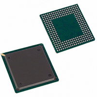
DS33R11+ Maxim Integrated Products, DS33R11+ Datasheet - Page 207

DS33R11+
Manufacturer Part Number
DS33R11+
Description
IC ETH TXRX T1/E1/J1 256-BGA
Manufacturer
Maxim Integrated Products
Type
Transceiverr
Datasheet
1.DS33R11.pdf
(344 pages)
Specifications of DS33R11+
Protocol
T1/E1/J1
Voltage - Supply
1.8V, 3.3V
Mounting Type
Surface Mount
Package / Case
256-BGA
Lead Free Status / RoHS Status
Lead free / RoHS Compliant
Number Of Drivers/receivers
-
- Current page: 207 of 344
- Download datasheet (12Mb)
Register Name:
Register Description:
Register Address:
Bit #
Name
Default
Bit 7: Transmit B8ZS Enable (TB8ZS)
Bit 6: Transmit SLC-96/Fs-Bit Insertion Enable (TSLC96). Only set this bit to a 1 in D4 framing applications.
Must be set to 1 to source the Fs pattern from the TR.TFDL register. See Section
Bit 5: Transmit FDL Zero-Stuffer Enable (TZSE). Set this bit to 0 if using the internal HDLC controller instead of
the legacy support for the FDL. See Section 15 for details.
Bit 4: F-Bit Corruption Type 2 (FBCT2). Setting this bit high enables the corruption of one Ft (D4 framing mode)
or FPS (ESF framing mode) bit in every 128 Ft or FPS bits as long as the bit remains set.
Bit 3: F-Bit Corruption Type 1 (FBCT1). A low-to-high transition of this bit causes the next three consecutive Ft
(D4 framing mode) or FPS (ESF framing mode) bits to be corrupted causing the remote end to experience a loss of
synchronization.
Bit 2: Transmit-Side D4 Yellow Alarm Select (TD4YM)
Bit 0: Transmit-Side Bit 7 Zero-Suppression Enable (TB7ZS)
0 = B8ZS disabled
1 = B8ZS enabled
0 = SLC-96/Fs-bit insertion disabled
1 = SLC-96/Fs-bit insertion enabled
0 = zero stuffer disabled
1 = zero stuffer enabled
0 = 0s in bit 2 of all channels
1 = a 1 in the S-bit position of frame 12
0 = no stuffing occurs
1 = bit 7 forced to a 1 in channels with all 0s
TB8ZS
7
0
TSLC96
TR.T1TCR2
T1 Transmit Control Register 2
06h
6
0
TZSE
5
0
207 of 344
FBCT2
0
4
FBCT1
3
0
TD4YM
2
0
10.18
for details.
—
1
0
TB7ZS
0
0
Related parts for DS33R11+
Image
Part Number
Description
Manufacturer
Datasheet
Request
R

Part Number:
Description:
MAX7528KCWPMaxim Integrated Products [CMOS Dual 8-Bit Buffered Multiplying DACs]
Manufacturer:
Maxim Integrated Products
Datasheet:

Part Number:
Description:
Single +5V, fully integrated, 1.25Gbps laser diode driver.
Manufacturer:
Maxim Integrated Products
Datasheet:

Part Number:
Description:
Single +5V, fully integrated, 155Mbps laser diode driver.
Manufacturer:
Maxim Integrated Products
Datasheet:

Part Number:
Description:
VRD11/VRD10, K8 Rev F 2/3/4-Phase PWM Controllers with Integrated Dual MOSFET Drivers
Manufacturer:
Maxim Integrated Products
Datasheet:

Part Number:
Description:
Highly Integrated Level 2 SMBus Battery Chargers
Manufacturer:
Maxim Integrated Products
Datasheet:

Part Number:
Description:
Current Monitor and Accumulator with Integrated Sense Resistor; ; Temperature Range: -40°C to +85°C
Manufacturer:
Maxim Integrated Products

Part Number:
Description:
TSSOP 14/A�/RS-485 Transceivers with Integrated 100O/120O Termination Resis
Manufacturer:
Maxim Integrated Products

Part Number:
Description:
TSSOP 14/A�/RS-485 Transceivers with Integrated 100O/120O Termination Resis
Manufacturer:
Maxim Integrated Products

Part Number:
Description:
QFN 16/A�/AC-DC and DC-DC Peak-Current-Mode Converters with Integrated Step
Manufacturer:
Maxim Integrated Products

Part Number:
Description:
TDFN/A/65V, 1A, 600KHZ, SYNCHRONOUS STEP-DOWN REGULATOR WITH INTEGRATED SWI
Manufacturer:
Maxim Integrated Products

Part Number:
Description:
Integrated Temperature Controller f
Manufacturer:
Maxim Integrated Products

Part Number:
Description:
SOT23-6/I�/45MHz to 650MHz, Integrated IF VCOs with Differential Output
Manufacturer:
Maxim Integrated Products

Part Number:
Description:
SOT23-6/I�/45MHz to 650MHz, Integrated IF VCOs with Differential Output
Manufacturer:
Maxim Integrated Products

Part Number:
Description:
EVALUATION KIT/2.4GHZ TO 2.5GHZ 802.11G/B RF TRANSCEIVER WITH INTEGRATED PA
Manufacturer:
Maxim Integrated Products

Part Number:
Description:
QFN/E/DUAL PCIE/SATA HIGH SPEED SWITCH WITH INTEGRATED BIAS RESISTOR
Manufacturer:
Maxim Integrated Products
Datasheet:


