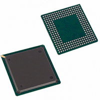
DS33R11+ Maxim Integrated Products, DS33R11+ Datasheet - Page 302

DS33R11+
Manufacturer Part Number
DS33R11+
Description
IC ETH TXRX T1/E1/J1 256-BGA
Manufacturer
Maxim Integrated Products
Type
Transceiverr
Datasheet
1.DS33R11.pdf
(344 pages)
Specifications of DS33R11+
Protocol
T1/E1/J1
Voltage - Supply
1.8V, 3.3V
Mounting Type
Surface Mount
Package / Case
256-BGA
Lead Free Status / RoHS Status
Lead free / RoHS Compliant
Number Of Drivers/receivers
-
- Current page: 302 of 344
- Download datasheet (12Mb)
In Half-Duplex (DTE) Mode, the DS33R11 supports CRS and COL signals. CRS is active when the PHY detects
transmit or receive activity. If there is a collision as indicated by the COL input, the DS33R11 will replace the data
nibbles with jam nibbles. After a “random“ time interval, the packet is retransmitted. The MAC will try to send the
packet a maximum of 16 times. The jam sequence consists of 55555555h. Note that the COL signal and CRS can
be asynchronous to the TX_CLK and are only valid in half duplex mode.
Figure 12-6. MII Transmit Half Duplex with a Collision Functional Timing
Receive Data (RXD[3:0]) is clocked from the external PHY synchronously with RX_CLK. The RX_CLK signal is
2.5MHz for 10Mbit/s operation and 25MHz for 100Mbit/s operation. RX_DV is asserted by the PHY from the first
nibble of the preamble in 100 Mbit/s operation or first nibble of SFD for 10 Mbit/s operation. The data on RXD[3:0]
is not accepted by the MAC if RX_DV is low or RX_ERR is high (in DTE mode). RX_ERR should be tied low when
in DCE Mode.
Figure 12-7. MII Receive Functional Timing
In RMII Mode, TX_EN is high with the first bit of the preamble. The TXD[1:0] is synchronous with the 50MHz
REF_CLK. For 10 Mbit/s operation, the data bit outputs are updated every 10 clocks.
Figure 12-8. RMII Transmit Interface Functional Timing
TXD[1:0]
TXD[3:0]
TX_EN
TX_EN
REFCLK
CRS
COL
TX_CLK
RX_CLK
RXD[3:0]
P
P
R
R
P
E
E
R
A
A
M
M
E
B
B
L
L
A
E
E
J
E
J
302 of 344
J
M
J
J
B
J
L
J
J
E
F
F
C
C
S
S
Related parts for DS33R11+
Image
Part Number
Description
Manufacturer
Datasheet
Request
R

Part Number:
Description:
MAX7528KCWPMaxim Integrated Products [CMOS Dual 8-Bit Buffered Multiplying DACs]
Manufacturer:
Maxim Integrated Products
Datasheet:

Part Number:
Description:
Single +5V, fully integrated, 1.25Gbps laser diode driver.
Manufacturer:
Maxim Integrated Products
Datasheet:

Part Number:
Description:
Single +5V, fully integrated, 155Mbps laser diode driver.
Manufacturer:
Maxim Integrated Products
Datasheet:

Part Number:
Description:
VRD11/VRD10, K8 Rev F 2/3/4-Phase PWM Controllers with Integrated Dual MOSFET Drivers
Manufacturer:
Maxim Integrated Products
Datasheet:

Part Number:
Description:
Highly Integrated Level 2 SMBus Battery Chargers
Manufacturer:
Maxim Integrated Products
Datasheet:

Part Number:
Description:
Current Monitor and Accumulator with Integrated Sense Resistor; ; Temperature Range: -40°C to +85°C
Manufacturer:
Maxim Integrated Products

Part Number:
Description:
TSSOP 14/A�/RS-485 Transceivers with Integrated 100O/120O Termination Resis
Manufacturer:
Maxim Integrated Products

Part Number:
Description:
TSSOP 14/A�/RS-485 Transceivers with Integrated 100O/120O Termination Resis
Manufacturer:
Maxim Integrated Products

Part Number:
Description:
QFN 16/A�/AC-DC and DC-DC Peak-Current-Mode Converters with Integrated Step
Manufacturer:
Maxim Integrated Products

Part Number:
Description:
TDFN/A/65V, 1A, 600KHZ, SYNCHRONOUS STEP-DOWN REGULATOR WITH INTEGRATED SWI
Manufacturer:
Maxim Integrated Products

Part Number:
Description:
Integrated Temperature Controller f
Manufacturer:
Maxim Integrated Products

Part Number:
Description:
SOT23-6/I�/45MHz to 650MHz, Integrated IF VCOs with Differential Output
Manufacturer:
Maxim Integrated Products

Part Number:
Description:
SOT23-6/I�/45MHz to 650MHz, Integrated IF VCOs with Differential Output
Manufacturer:
Maxim Integrated Products

Part Number:
Description:
EVALUATION KIT/2.4GHZ TO 2.5GHZ 802.11G/B RF TRANSCEIVER WITH INTEGRATED PA
Manufacturer:
Maxim Integrated Products

Part Number:
Description:
QFN/E/DUAL PCIE/SATA HIGH SPEED SWITCH WITH INTEGRATED BIAS RESISTOR
Manufacturer:
Maxim Integrated Products
Datasheet:


