COM20022I3V-HT SMSC, COM20022I3V-HT Datasheet - Page 76
COM20022I3V-HT
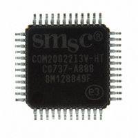
Manufacturer Part Number
COM20022I3V-HT
Description
IC CTRLR ARCNET 2KX8 RAM 48-TQFP
Manufacturer
SMSC
Series
ARCNETr
Datasheet
1.COM20022I3V-HT.pdf
(82 pages)
Specifications of COM20022I3V-HT
Controller Type
ARCNET Controller
Interface
Differential
Voltage - Supply
4.5 V ~ 5.5 V
Current - Supply
65mA
Operating Temperature
-40°C ~ 85°C
Mounting Type
Surface Mount
Package / Case
48-TQFP, 48-VQFP
Lead Free Status / RoHS Status
Lead free / RoHS Compliant
Other names
638-1004
Available stocks
Company
Part Number
Manufacturer
Quantity
Price
Company:

Part Number:
COM20022I3V-HT
Manufacturer:
Standard
Quantity:
2 784
Company:
Part Number:
COM20022I3V-HT
Manufacturer:
AD
Quantity:
7 439
Company:
Part Number:
COM20022I3V-HT
Manufacturer:
Microchip Technology
Quantity:
10 000
Part Number:
COM20022I3V-HT
Manufacturer:
SMSC
Quantity:
20 000


Notes:
1.
2.
3.
Revision 09-27-07
t10
t11
t12
t13
t14
t15
t16
t17
t18
t19
t20
t21
t22
t23
t24
t25
t26
t1
t2
t3
t4
t5
t6
t7
t8
t9
Tarb is the ARBITRATION CLOCK PERIOD. It depends on Topr and SLOWARB bit.
SLOWARB must set to “1” if the data rate is over 5 Mbps. (i.e. 10 Mbps)
Tarb is Topr at SLOWARB=0 and Tarb is 2Topr at SLOWARB=1.
Topr is the period of Operation Clock Frequency. It depends on the CKUP1 and CKUP0 bits.
Txtl is a period of external XTAL oscillation frequency.
The nREFEX pin must not be Low while nDACK is Low.
nDACK Inactive Pulse Width
The First DREQ Assertion Delay After Writing Low
Pointer
DREQ Assert Delay from nREFEX Active at
Programmable Burst Transfer Mode
DREQ Assertion Delay from Write/Read Inactive at Non-
Burst Transfer Mode
DREQ Assertion Delay from nDACK
Inactive due to Timeout of Gate Timer
at Programmable Burst Transfer Mode
DREQ Negation Delay from Write/Read Active
DREQ Negation Delay from TC and Write/Read Active
Data Access Time from Read Active
Data Float Delay from Read Inactive
nREFEX Active Pulse Width
Write Active Pulse Width
Read Active Pulse Width
Active Pulse Overlap Width between TC and Write/Read
Write/Read Inactive Pulse Width
Write Cycle Interval Period
Read Cycle Interval Period
Data Setup to Write Inactive
Data Hold From Write Inactive
nCS High Setup to nDACK Active
nCS High Hold from nDACK Inactive
DREQ Active Setup to nDACK Active
DIR Setup to nDS Low (Motorola mode only)
DIR Hold from nDS High (Motorola mode only)
nDACK Setup to Write/Read Active
nDACK Hold After Write/Read Inactive
nREFEX Inactive Time
PARAMETER
DATASHEET
Table 8.1 - DMA Timing
CASE1w/1R
CASE2w/2R
GTTM bit=1
CASE 1W
CASE 2W
CASE 1R
CASE 2R
CASE1R
CASE2R
Page 76
GTTM
bit =0
10 Mbps ARCNET (ANSI 878.1) Controller with 2Kx8 On-Chip RAM
4Tarb+3
4 Tarb
4Tarb
4Tarb
15Txtl
7Txtl
3Txtl
MIN
100
0nS
20
20
65
60
20
20
30
30
10
20
20
20
10
10
30
0
0
0
0
0
5
Tarb
TYP
5
+40ns
5Tarb
+40ns
+40ns
16Txtl
MAX
8Txtl
30
40
40
40
40
40
20
UNIT
ns
ns
ns
ns
ns
ns
ns
ns
ns
ns
ns
ns
ns
ns
ns
ns
ns
ns
ns
ns
ns
ns
ns
ns
SMSC COM20022I
Note 1
Note 3
Note 4
Note 2
Note 4
Note 4
Note 4
Note 4
Note 4
Note 4
Note 4
Note 4
Note 4
Note 2
Datasheet
NOTE
1,4,5
Note
Note
Note
Note
Note
4,5
4,5
4,5
1,4
Related parts for COM20022I3V-HT
Image
Part Number
Description
Manufacturer
Datasheet
Request
R

Part Number:
Description:
IC CTRLR ARCNET 2KX8 RAM 48-TQFP
Manufacturer:
SMSC
Datasheet:

Part Number:
Description:
10 Mbps ARCNET (ANSI 878.1) Controller with 2Kx8 On-Board RAM
Manufacturer:
SMSC [SMSC Corporation]
Part Number:
Description:
10 Mbps ARCNET (ANSI 878.1) Controller with 2Kx8 On-Chip RAM
Manufacturer:
SMSC Corporation
Part Number:
Description:
FAST ETHERNET PHYSICAL LAYER DEVICE
Manufacturer:
SMSC Corporation
Datasheet:
Part Number:
Description:
357-036-542-201 CARDEDGE 36POS DL .156 BLK LOPRO
Manufacturer:
SMSC Corporation
Datasheet:
Part Number:
Description:
357-036-542-201 CARDEDGE 36POS DL .156 BLK LOPRO
Manufacturer:
SMSC Corporation
Datasheet:
Part Number:
Description:
357-036-542-201 CARDEDGE 36POS DL .156 BLK LOPRO
Manufacturer:
SMSC Corporation
Datasheet:
Part Number:
Description:
4-PORT USB2.0 HUB CONTROLLER
Manufacturer:
SMSC Corporation
Datasheet:
Part Number:
Description:
Manufacturer:
SMSC Corporation
Datasheet:
Part Number:
Description:
Manufacturer:
SMSC Corporation
Datasheet:
Part Number:
Description:
FDC37C672ENHANCED SUPER I/O CONTROLLER WITH FAST IR
Manufacturer:
SMSC Corporation
Datasheet:
Part Number:
Description:
COM90C66LJPARCNET Controller/Transceiver with AT Interface and On-Chip RAM
Manufacturer:
SMSC Corporation
Datasheet:
Part Number:
Description:
Manufacturer:
SMSC Corporation
Datasheet:
Part Number:
Description:
Manufacturer:
SMSC Corporation
Datasheet: