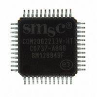
COM20022I3V-HT SMSC, COM20022I3V-HT Datasheet - Page 25

COM20022I3V-HT
Manufacturer Part Number
COM20022I3V-HT
Description
IC CTRLR ARCNET 2KX8 RAM 48-TQFP
Manufacturer
SMSC
Series
ARCNETr
Datasheet
1.COM20022I3V-HT.pdf
(82 pages)
Specifications of COM20022I3V-HT
Controller Type
ARCNET Controller
Interface
Differential
Voltage - Supply
4.5 V ~ 5.5 V
Current - Supply
65mA
Operating Temperature
-40°C ~ 85°C
Mounting Type
Surface Mount
Package / Case
48-TQFP, 48-VQFP
Lead Free Status / RoHS Status
Lead free / RoHS Compliant
Other names
638-1004
Available stocks
Company
Part Number
Manufacturer
Quantity
Price
Company:
Part Number:
COM20022I3V-HT
Manufacturer:
Standard
Quantity:
2 784
Company:
Part Number:
COM20022I3V-HT
Manufacturer:
AD
Quantity:
7 439
Company:
Part Number:
COM20022I3V-HT
Manufacturer:
Microchip Technology
Quantity:
10 000
Part Number:
COM20022I3V-HT
Manufacturer:
SMSC
Quantity:
20 000
10 Mbps ARCNET (ANSI 878.1) Controller with 2Kx8 On-Chip RAM
Datasheet
5.2
SMSC COM20022I
BUSTMG PIN
Sampled A2-A0, nCS
0
1
1
More delayed nRD
The I/O address and Chip Select signals, which are supplied to the data output logic, are not sampled.
Also, the nRD signal is not delayed, because the above sampling and delaying paths decrease the data
access time of the read cycle.
The above sampling and delaying signals are supplied to the Read Pulse Generation logic which
generates the clearing pulse for the Diagnostic register and generates the starting pulse of the RAM
Arbitration. Typical delay time between nRD and nRD1 is around 15nS and between nRD1 and nRD2 is
around 10nS.
Longer pulse widths are needed due to these delays on nRD signal. However, the CPU can insert some
wait cycles to extend the width without any impact on performance.
The BUSTMG pin is used to support this function. It is used to Enable/Disable the High Speed CPU Read
and Write function. It is defined as: BUSTMG = 0, the High Speed CPU Read and Write operations are
enabled; BUSTMG = 1, the High Speed CPU Read and Write operations are disabled if the RBUSTMG bit
is 0. If BUSTMG = 1 and RBUSTMG = 1, High Speed CPU Read operations are enabled (see definition of
RBUSTMG bit below).
The RBUSTMG bit was added to Disable/Enable the High Speed CPU Read function. It is defined as:
RBUSTMG=0, Disabled (Default); RBUSTMG=1, Enabled.
In the MOTOROLA CPU mode (DIR, nDS mode), the same modifications apply.
Transmission Media Interface
The bottom halves of Figure 5.1 and Figure 5.2 illustrate the COM20022I interface to the transmission
media used to connect the node to the network. Table 5.1 lists different types of cable which are suitable
for ARCNET applications. The user may interface to the cable of choice in one of three ways:
Delayed nRD
(nRD2)
A2-A0, nCS
(nRD1)
nRD
Figure 5.7
RBUSTMG BIT
X
0
1
- High Speed CPU Bus Timing - Intel CPU Mode
DATASHEET
High Speed CPU Read and Write
Normal Speed CPU Read and Write
High Speed CPU Read and Normal Speed CPU Write
Page 25
VALID
VALID
BUS TIMING MODE
Revision 09-27-07


