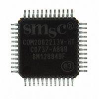
COM20022I3V-HT SMSC, COM20022I3V-HT Datasheet - Page 20

COM20022I3V-HT
Manufacturer Part Number
COM20022I3V-HT
Description
IC CTRLR ARCNET 2KX8 RAM 48-TQFP
Manufacturer
SMSC
Series
ARCNETr
Datasheet
1.COM20022I3V-HT.pdf
(82 pages)
Specifications of COM20022I3V-HT
Controller Type
ARCNET Controller
Interface
Differential
Voltage - Supply
4.5 V ~ 5.5 V
Current - Supply
65mA
Operating Temperature
-40°C ~ 85°C
Mounting Type
Surface Mount
Package / Case
48-TQFP, 48-VQFP
Lead Free Status / RoHS Status
Lead free / RoHS Compliant
Other names
638-1004
Available stocks
Company
Part Number
Manufacturer
Quantity
Price
Company:
Part Number:
COM20022I3V-HT
Manufacturer:
Standard
Quantity:
2 784
Company:
Part Number:
COM20022I3V-HT
Manufacturer:
AD
Quantity:
7 439
Company:
Part Number:
COM20022I3V-HT
Manufacturer:
Microchip Technology
Quantity:
10 000
Part Number:
COM20022I3V-HT
Manufacturer:
SMSC
Quantity:
20 000
5.1.3
Revision 09-27-07
only or by either internal or external TC. ITCEN is for Non-Burst or Burst mode. RTRG selects the re-
trigger mode as either external or internal. It is for the two Programmable-Burst modes.
The TC8/RSYN/GTTM bit has one of three functions, depending on the DMA transfer mode selected. TC8
is bit 8 of the Terminal Count. It is the MSB of the 9 bit Terminal Count setting register (the other 8 bits are
in the DMA Count register). TC8 is for Non-Burst or Burst mode. RSYN is the Refresh Synchronous bit.
This bit is used to select whether the DMA is started immediately or after Refresh execution. GTTM is the
Gate Time bit. This bit selects whether the Gate Time is 350nS (min) or 750nS (min). RSYN and GTTM
are for the two Programmable-Burst modes. RSYN is for External Re-Trigger mode; GTTM is for internal
Re-Trigger mode.
Located in the DMA Count Register, the TC7-TC0 /TIM7-TIM0 /CYC7-CYC0 bits have one of three
functions depending on the DMA transfer mode. TC7-TC0 are for non-burst or burst mode. These are the
lower 8 bits of the Terminal Count setting register (the MSB is in the Bus Control Register). The TIM7-
TIM0 bits are for setting the time of the continuous DMA transfer in Programmable-Burst by Timer mode.
The CYC7-CYC0 bits are for setting the time of the continuous DMA transfer in Programmable-Burst by
Cycle mode.
DMA Operation
The DMA interface operates in one of four transfer modes: Non-Burst, Burst, Programmable-Burst (by
timer) and Programmable-Burst (by cycle counter). The data transfer mode of the DMA is selected through
the DMAMD[1,0] bits in the Bus Control register, bits [3,2]. These modes are described below.
Non-Burst mode is a Single Transfer mode wherein, the DREQ pin is asserted after writing the Address
Pointer Low Register when DMAEN=1. Actually, DREQ pin is asserted 4T
Address Pointer Low Register when DMAEN = 1 (refer to Figure 5.3). This mode operates as follows:
1.
2.
3.
4.
Repeat above 4 steps until the TC pin goes active. This mode is called "Cycle steal mode".
Burst mode is a Demand Transfer mode. In this mode, the DREQ pin is asserted after writing the Address
Pointer Low Register when DMAEN=1. Actually, DREQ pin is asserted 4T
Address Pointer Low Register when DMAEN = 1 (refer to Figure 5.3). The DACK pin is asserted by the
DMA Controller detecting the DREQ pin asserted. The DREQ pin stays asserted until the TC pin goes
High.
Programmable-Burst mode is a Demand Transfer mode with temporary DREQ deassertion for a Refresh
cycle. The DREQ pin is asserted after writing the Address Pointer Low Register when DMAEN=1 (refer to
Figure 5.3). The DACK pin is asserted by the DMA Controller detecting the DREQ pin asserted. If the
continuous DMA operation time is longer than the set Refresh period, then DREQ is deasserted. The
DREQ is held deasserted after negating nDACK for the Gate time. After the Gate time, the DREQ pin is
asserted again. The DREQ pin stays asserted until the TC pin goes High. In Programmable-Burst mode,
the gating can be by timer or by cycle counter.
The nDACK pin is asserted by the DMA Controller detecting the DREQ pin asserted.
The DREQ pin is deasserted by the COM20022I detecting the nDACK pin asserted.
The nDACK pin is deasserted by the DMA Controller detecting the DREQ pin deasserted after
executing the present read or write cycle.
The DREQ pin is asserted by the COM20022I detecting the DACK pin deasserted.
DATASHEET
Page 20
10 Mbps ARCNET (ANSI 878.1) Controller with 2Kx8 On-Chip RAM
ARB
ARB
time after writing the
time after writing the
SMSC COM20022I
Datasheet


