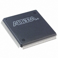
EP20K100QC240-3 Altera, EP20K100QC240-3 Datasheet - Page 54

EP20K100QC240-3
Manufacturer Part Number
EP20K100QC240-3
Description
IC APEX 20K FPGA 100K 240-PQFP
Manufacturer
Altera
Series
APEX-20K®r
Datasheet
1.EP20K30ETC144-3.pdf
(117 pages)
Specifications of EP20K100QC240-3
Number Of Logic Elements/cells
4160
Number Of Labs/clbs
416
Total Ram Bits
53248
Number Of I /o
189
Number Of Gates
263000
Voltage - Supply
2.375 V ~ 2.625 V
Mounting Type
Surface Mount
Operating Temperature
0°C ~ 85°C
Package / Case
240-MQFP, 240-PQFP
Lead Free Status / RoHS Status
Contains lead / RoHS non-compliant
Other names
544-1094
Available stocks
Company
Part Number
Manufacturer
Quantity
Price
Company:
Part Number:
EP20K100QC240-3N
Manufacturer:
ALTERA
Quantity:
150
Part Number:
EP20K100QC240-3V
Manufacturer:
ALTERA/阿尔特拉
Quantity:
20 000
APEX 20K Programmable Logic Device Family Data Sheet
54
Notes to
(1)
(2)
(3)
(4)
SignalTap
Embedded
Logic Analyzer
f
IN
Table 18. APEX 20KE Clock Input & Output Parameters
Symbol
All input clock specifications must be met. The PLL may not lock onto an incoming clock if the clock specifications
are not met, creating an erroneous clock within the device.
The maximum lock time is 40 µs or 2000 input clock cycles, whichever occurs first.
Before configuration, the PLL circuits are disable and powered down. During configuration, the PLLs are still
disabled. The PLLs begin to lock once the device is in the user mode. If the clock enable feature is used, lock begins
once the CLKLK_ENA pin goes high in user mode.
The PLL VCO operating range is 200 MHz ð f
Tables 17
Input clock frequency
and 18:
Parameter
APEX 20K devices include device enhancements to support the SignalTap
embedded logic analyzer. By including this circuitry, the APEX 20K
device provides the ability to monitor design operation over a period of
time through the IEEE Std. 1149.1 (JTAG) circuitry; a designer can analyze
internal logic at speed without bringing internal signals to the I/O pins.
This feature is particularly important for advanced packages such as
FineLine BGA packages because adding a connection to a pin during the
debugging process can be difficult after a board is designed and
manufactured.
SSTL-2 Class
SSTL-2 Class
SSTL-3 Class
SSTL-3 Class
I/O Standard
3.3-V LVTTL
2.5-V LVTTL
1.8-V LVTTL
LVDS
GTL+
VCO
II
II
I
I
ð 840 MHz for LVDS mode.
-1X Speed Grade
(Part 2 of 2)
Min
1.5
1.5
1.5
1.5
1.5
1.5
1.5
1.5
1.5
Max
290
281
272
303
291
291
300
300
420
Note (1)
-2X Speed Grade
Min
1.5
1.5
1.5
1.5
1.5
1.5
1.5
1.5
1.5
Altera Corporation
Max
257
250
243
261
253
253
260
260
350
Units
MHz
MHz
MHz
MHz
MHz
MHz
MHz
MHz
MHz


