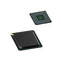
LPC1850FET256,551 NXP Semiconductors, LPC1850FET256,551 Datasheet - Page 27

LPC1850FET256,551
Manufacturer Part Number
LPC1850FET256,551
Description
MCU 32BIT ARM CORTEX M3 256BGA
Manufacturer
NXP Semiconductors
Series
LPC18xxr
Datasheet
1.LPC1830FET256551.pdf
(87 pages)
Specifications of LPC1850FET256,551
Core Processor
ARM® Cortex-M3™
Core Size
32-Bit
Speed
150MHz
Connectivity
CAN, EBI/EMI, Ethernet, I²C, IrDA, Microwire, QEI, SD/MMC, SPI, SSI, SSP, UART/USART, USB, USB OTG
Peripherals
Brown-out Detect/Reset, DMA, I²S, LCD, POR, PWM, WDT
Number Of I /o
80
Program Memory Size
-
Program Memory Type
ROMless
Eeprom Size
-
Ram Size
200K x 8
Voltage - Supply (vcc/vdd)
2.2 V ~ 3.6 V
Data Converters
A/D 8x10b; D/A 1x10b
Oscillator Type
Internal
Operating Temperature
-40°C ~ 85°C
Package / Case
256-LBGA
Processor Series
LPC1850
Core
ARM Cortex M3
Data Bus Width
32 bit
Data Ram Size
200 KB
Interface Type
SPI Flash (SPIFI), USB, Ethernet, LCD, External Memory Controller, I2C
Maximum Clock Frequency
150 MHz
Number Of Programmable I/os
80
Number Of Timers
6
Operating Supply Voltage
2 V to 3.6 V
Maximum Operating Temperature
+ 85 C
Mounting Style
SMD/SMT
Minimum Operating Temperature
- 40 C
Operating Temperature Range
- 40 C to + 85 C
Lead Free Status / Rohs Status
Lead free / RoHS Compliant
Other names
568-6682
Available stocks
Company
Part Number
Manufacturer
Quantity
Price
Company:
Part Number:
LPC1850FET256,551
Manufacturer:
NXP Semiconductors
Quantity:
10 000
Part Number:
LPC1850FET256,551
Manufacturer:
NXP/恩智浦
Quantity:
20 000
NXP Semiconductors
Table 3.
LPC1850_30_20_10
Objective data sheet
Symbol
TDI
I
I2C0_SCL
I2C0_SDA
USB0 pins
USB0_DP
USB0_DM
USB0_VBUS
USB0_ID
USB0_RREF
USB1 pins
USB1_DP
USB1_DM
Reset and wake-up pins
RESET
WAKEUP0
WAKEUP1
WAKEUP2
WAKEUP3
ADC pins
ADC0
ADC1
ADC2
ADC3
ADC4
ADC5
ADC6
ADC7
RTC
RTC_ALARM
RTCX1
RTCX2
2
C-bus pins
[2]
[6]
[6]
[6]
[6]
[6]
[6]
[6]
[6]
[9]
[6]
[5]
[7]
[8]
[8]
[5]
[7]
Pin description
[5]
[6]
J4
L15
L16
F2
G2
F1
H2
H1
F12
G12 -
D9
A9
A10
C9
D8
E3
C3
A4
B5
C6
B3
A5
C5
A11
A8
B8
…continued
Reset
state
[1]
I; PU
I; F
I; F
-
-
-
-
-
-
I; IA
I; IA
I; IA
I; IA
I; IA
I; IA
I; IA
I; IA
I; IA
I; IA
I; IA
I; IA
I; IA
-
-
-
Type Description
I
I/O
I/O
I/O
I/O
I/O
I
-
I/O
I/O
I
I
I
I
I
-
-
-
-
-
-
-
-
-
-
-
All information provided in this document is subject to legal disclaimers.
Test Data In for JTAG interface.
I
I
USB0 bidirectional D+ line.
USB0 bidirectional D line.
VBUS pin (power on USB cable).
Indicates to the transceiver whether connected a A-device (ID LOW) or
B-device (ID HIGH).
USB connection for external reference resistor (12.0 k 1 %) to analog
ground supply.
USB1 bidirectional D+ line.
USB1 bidirectional D line.
External reset input: A LOW on this pin resets the device, causing I/O ports
and peripherals to take on their default states, and processor execution to
begin at address 0.
External wake-up input; can raise an interrupt and can cause wake-up from
any of the low power modes.
External wake-up input; can raise an interrupt and can cause wake-up from
any of the low power modes.
External wake-up input; can raise an interrupt and can cause wake-up from
any of the low power modes.
External wake-up input; can raise an interrupt and can cause wake-up from
any of the low power modes.
ADC0/1 input channel 0. Shared between ADC0, ADC1, and DAC.
ADC0/1 input channel 1.
ADC0/1 input channel 2.
ADC0/1 input channel 3.
ADC0/1 input channel 4.
ADC0/1 input channel 5.
ADC0/1 input channel 6.
ADC0/1 input channel 7.
RTC controlled output.
Input to the RTC 32 kHz ultra-low power oscillator circuit.
Output from the RTC 32 kHz ultra-low power oscillator circuit.
2
2
C clock input/output. Open-drain output (for I
C data input/output. Open-drain output (for I
Rev. 1.2 — 17 February 2011
32-bit ARM Cortex-M3 microcontroller
LPC1850/30/20/10
2
2
C-bus compliance).
C-bus compliance).
© NXP B.V. 2011. All rights reserved.
27 of 87


