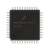
MC9S08AW60CFGE Freescale, MC9S08AW60CFGE Datasheet - Page 98

MC9S08AW60CFGE
Manufacturer Part Number
MC9S08AW60CFGE
Description
Manufacturer
Freescale
Datasheet
1.MC9S08AW60CFGE.pdf
(336 pages)
Specifications of MC9S08AW60CFGE
Cpu Family
HCS08
Device Core Size
8b
Frequency (max)
40MHz
Interface Type
I2C/SCI/SPI
Total Internal Ram Size
2KB
# I/os (max)
34
Number Of Timers - General Purpose
8
Operating Supply Voltage (typ)
3.3/5V
Operating Supply Voltage (max)
5.5V
Operating Supply Voltage (min)
2.7V
On-chip Adc
8-chx10-bit
Instruction Set Architecture
CISC
Operating Temp Range
-40C to 85C
Operating Temperature Classification
Industrial
Mounting
Surface Mount
Pin Count
44
Package Type
LQFP
Program Memory Type
Flash
Program Memory Size
60KB
Lead Free Status / RoHS Status
Compliant
Available stocks
Company
Part Number
Manufacturer
Quantity
Price
Company:
Part Number:
MC9S08AW60CFGE
Manufacturer:
Freescale Semiconductor
Quantity:
10 000
Company:
Part Number:
MC9S08AW60CFGER
Manufacturer:
Freescale Semiconductor
Quantity:
10 000
- Current page: 98 of 336
- Download datasheet (7Mb)
1
1
Chapter 6 Parallel Input/Output
6.7.8
In addition to the I/O control, port D pins are controlled by the registers listed below.
98
PTDPE[3:0]
PTDSE[3:0]
Bits 7 through 4 are reserved bits that must always be written to 0.
Bits 7 through 4 are reserved bits that must always be written to 0.
Reset
Reset
Field
Field
3:0
3:0
W
W
R
R
Port D Pin Control Registers (PTDPE, PTDSE, PTDDS)
Internal Pullup Enable for Port D Bits — Each of these control bits determines if the internal pullup device is
enabled for the associated PTD pin. For port D pins that are configured as outputs, these bits have no effect and
the internal pullup devices are disabled.
0 Internal pullup device disabled for port D bit n.
1 Internal pullup device enabled for port D bit n.
Output Slew Rate Control Enable for Port D Bits — Each of these control bits determine whether output slew
rate control is enabled for the associated PTD pin. For port D pins that are configured as inputs, these bits have
no effect.
0 Output slew rate control disabled for port D bit n.
1 Output slew rate control enabled for port D bit n.
R
R
0
0
7
7
Figure 6-28. Output Slew Rate Control Enable for Port D (PTDSE)
Figure 6-27. Internal Pullup Enable for Port D (PTDPE)
R
R
0
0
6
6
Table 6-18. PTDPE Register Field Descriptions
Table 6-19. PTDSE Register Field Descriptions
MC9S08AC16 Series Data Sheet, Rev. 8
R
R
0
0
5
5
R
R
0
0
4
4
Description
Description
PTDPE3
PTDSE3
3
0
3
0
PTDPE2
PTDSE2
0
0
2
2
1
PTDPE1
PTDSE1
1
Freescale Semiconductor
0
0
1
1
PTDPE0
PTDSE0
0
0
0
0
Related parts for MC9S08AW60CFGE
Image
Part Number
Description
Manufacturer
Datasheet
Request
R

Part Number:
Description:
TOWER ELEVATOR BOARDS HARDWARE
Manufacturer:
Freescale Semiconductor
Datasheet:

Part Number:
Description:
TOWER SERIAL I/O HARDWARE
Manufacturer:
Freescale Semiconductor
Datasheet:

Part Number:
Description:
LCD MODULE FOR TWR SYSTEM
Manufacturer:
Freescale Semiconductor
Datasheet:

Part Number:
Description:
DAUGHTER LCD WVGA I.MX51
Manufacturer:
Freescale Semiconductor
Datasheet:

Part Number:
Description:
TOWER SYSTEM BOARD MPC5125
Manufacturer:
Freescale Semiconductor
Datasheet:

Part Number:
Description:
KIT EVALUATION I.MX51
Manufacturer:
Freescale Semiconductor
Datasheet:

Part Number:
Description:
KIT DEVELOPMENT WINCE IMX25
Manufacturer:
Freescale Semiconductor
Datasheet:

Part Number:
Description:
TOWER SYSTEM KIT MPC5125
Manufacturer:
Freescale Semiconductor
Datasheet:

Part Number:
Description:
TOWER SYSTEM BOARD K40X256
Manufacturer:
Freescale Semiconductor
Datasheet:

Part Number:
Description:
TOWER SYSTEM KIT K40X256
Manufacturer:
Freescale Semiconductor
Datasheet:

Part Number:
Description:
Microcontrollers (MCU) MX28 PLATFORM DEV KIT
Manufacturer:
Freescale Semiconductor
Datasheet:

Part Number:
Description:
MCU, MPU & DSP Development Tools IAR KickStart Kit for Kinetis K60
Manufacturer:
Freescale Semiconductor
Datasheet:

Part Number:
Description:
24BIT HDMI MX535/08
Manufacturer:
Freescale Semiconductor
Datasheet:
Part Number:
Description:
Manufacturer:
Freescale Semiconductor, Inc
Datasheet:
Part Number:
Description:
Manufacturer:
Freescale Semiconductor, Inc
Datasheet:


