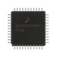
MC9S08AW60CFGE Freescale, MC9S08AW60CFGE Datasheet - Page 34

MC9S08AW60CFGE
Manufacturer Part Number
MC9S08AW60CFGE
Description
Manufacturer
Freescale
Datasheet
1.MC9S08AW60CFGE.pdf
(336 pages)
Specifications of MC9S08AW60CFGE
Cpu Family
HCS08
Device Core Size
8b
Frequency (max)
40MHz
Interface Type
I2C/SCI/SPI
Total Internal Ram Size
2KB
# I/os (max)
34
Number Of Timers - General Purpose
8
Operating Supply Voltage (typ)
3.3/5V
Operating Supply Voltage (max)
5.5V
Operating Supply Voltage (min)
2.7V
On-chip Adc
8-chx10-bit
Instruction Set Architecture
CISC
Operating Temp Range
-40C to 85C
Operating Temperature Classification
Industrial
Mounting
Surface Mount
Pin Count
44
Package Type
LQFP
Program Memory Type
Flash
Program Memory Size
60KB
Lead Free Status / RoHS Status
Compliant
Available stocks
Company
Part Number
Manufacturer
Quantity
Price
Company:
Part Number:
MC9S08AW60CFGE
Manufacturer:
Freescale Semiconductor
Quantity:
10 000
Company:
Part Number:
MC9S08AW60CFGER
Manufacturer:
Freescale Semiconductor
Quantity:
10 000
- Current page: 34 of 336
- Download datasheet (7Mb)
Chapter 2 Pins and Connections
2.3.7
The remaining pins are shared among general-purpose I/O and on-chip peripheral functions such as timers
and serial I/O systems. Immediately after reset, all of these pins are configured as high-impedance
general-purpose inputs with internal pullup devices disabled.
For information about controlling these pins as general-purpose I/O pins, see
Input/Output.” For information about how and when on-chip peripheral systems use these pins, refer to the
appropriate chapter from
When an on-chip peripheral system is controlling a pin, data direction control bits still determine what is
read from port data registers even though the peripheral module controls the pin direction by controlling
the enable for the pin’s output buffer. See the
Pullup enable bits for each input pin control whether on-chip pullup devices are enabled whenever the pin
is acting as an input even if it is being controlled by an on-chip peripheral module. When the PTD3, PTD2,
and PTG4 pins are controlled by the KBI module and are configured for rising-edge/high-level sensitivity,
the pullup enable control bits enable pulldown devices rather than pullup devices. Similarly, when IRQ is
configured as the IRQ input and is set to detect rising edges, the pullup enable control bit enables a
pulldown device rather than a pullup device.
34
General-Purpose I/O and Peripheral Ports
To avoid extra current drain from floating input pins, the reset initialization
routine in the application program should either enable on-chip pullup
devices or change the direction of unused pins to outputs so the pins do not
float.
When an alternative function is first enabled it is possible to get a spurious
edge to the module, user software should clear out any associated flags
before interrupts are enabled.
modules are enabled. The highest priority module will have control over the
pin. Selecting a higher priority pin function with a lower priority function
already enabled can cause spurious edges to the lower priority module. It is
recommended that all modules that share a pin be disabled before enabling
another module.
Table
2-2.
MC9S08AC16 Series Data Sheet, Rev. 8
Table 2-1
Chapter 6, “Parallel
NOTE
NOTE
illustrates the priority if multiple
Input/Output” chapter for more details.
Chapter 6, “Parallel
Freescale Semiconductor
Related parts for MC9S08AW60CFGE
Image
Part Number
Description
Manufacturer
Datasheet
Request
R

Part Number:
Description:
TOWER ELEVATOR BOARDS HARDWARE
Manufacturer:
Freescale Semiconductor
Datasheet:

Part Number:
Description:
TOWER SERIAL I/O HARDWARE
Manufacturer:
Freescale Semiconductor
Datasheet:

Part Number:
Description:
LCD MODULE FOR TWR SYSTEM
Manufacturer:
Freescale Semiconductor
Datasheet:

Part Number:
Description:
DAUGHTER LCD WVGA I.MX51
Manufacturer:
Freescale Semiconductor
Datasheet:

Part Number:
Description:
TOWER SYSTEM BOARD MPC5125
Manufacturer:
Freescale Semiconductor
Datasheet:

Part Number:
Description:
KIT EVALUATION I.MX51
Manufacturer:
Freescale Semiconductor
Datasheet:

Part Number:
Description:
KIT DEVELOPMENT WINCE IMX25
Manufacturer:
Freescale Semiconductor
Datasheet:

Part Number:
Description:
TOWER SYSTEM KIT MPC5125
Manufacturer:
Freescale Semiconductor
Datasheet:

Part Number:
Description:
TOWER SYSTEM BOARD K40X256
Manufacturer:
Freescale Semiconductor
Datasheet:

Part Number:
Description:
TOWER SYSTEM KIT K40X256
Manufacturer:
Freescale Semiconductor
Datasheet:

Part Number:
Description:
Microcontrollers (MCU) MX28 PLATFORM DEV KIT
Manufacturer:
Freescale Semiconductor
Datasheet:

Part Number:
Description:
MCU, MPU & DSP Development Tools IAR KickStart Kit for Kinetis K60
Manufacturer:
Freescale Semiconductor
Datasheet:

Part Number:
Description:
24BIT HDMI MX535/08
Manufacturer:
Freescale Semiconductor
Datasheet:
Part Number:
Description:
Manufacturer:
Freescale Semiconductor, Inc
Datasheet:
Part Number:
Description:
Manufacturer:
Freescale Semiconductor, Inc
Datasheet:


