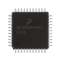
MC9S08AW60CFGE Freescale, MC9S08AW60CFGE Datasheet - Page 131

MC9S08AW60CFGE
Manufacturer Part Number
MC9S08AW60CFGE
Description
Manufacturer
Freescale
Datasheet
1.MC9S08AW60CFGE.pdf
(336 pages)
Specifications of MC9S08AW60CFGE
Cpu Family
HCS08
Device Core Size
8b
Frequency (max)
40MHz
Interface Type
I2C/SCI/SPI
Total Internal Ram Size
2KB
# I/os (max)
34
Number Of Timers - General Purpose
8
Operating Supply Voltage (typ)
3.3/5V
Operating Supply Voltage (max)
5.5V
Operating Supply Voltage (min)
2.7V
On-chip Adc
8-chx10-bit
Instruction Set Architecture
CISC
Operating Temp Range
-40C to 85C
Operating Temperature Classification
Industrial
Mounting
Surface Mount
Pin Count
44
Package Type
LQFP
Program Memory Type
Flash
Program Memory Size
60KB
Lead Free Status / RoHS Status
Compliant
Available stocks
Company
Part Number
Manufacturer
Quantity
Price
Company:
Part Number:
MC9S08AW60CFGE
Manufacturer:
Freescale Semiconductor
Quantity:
10 000
Company:
Part Number:
MC9S08AW60CFGER
Manufacturer:
Freescale Semiconductor
Quantity:
10 000
- Current page: 131 of 336
- Download datasheet (7Mb)
8.1.3
Figure 8-3
(ICG) module. This section includes a general description and a feature list.
8.2
The oscillator pins are used to provide an external clock source for the MCU. The oscillator pins are gain
controlled in low-power mode (default). Oscillator amplitudes in low-power mode are limited to
approximately 1 V, peak-to-peak.
8.2.1
If upon the first write to ICGC1, either the FEE mode or FBE mode is selected, this pin functions as either
the external clock input or the input of the oscillator circuit as determined by REFS. If upon the first write
to ICGC1, either the FEI mode or SCM mode is selected, this pin is not used by the ICG.
8.2.2
If upon the first write to ICGC1, either the FEE mode or FBE mode is selected, this pin functions as the
output of the oscillator circuit. If upon the first write to ICGC1, either the FEI mode or SCM mode is
selected, this pin is not used by the ICG. The oscillator is capable of being configured to provide a higher
amplitude output for improved noise immunity. This mode of operation is selected by HGO = 1.
Freescale Semiconductor
External Signal Description
is a top-level diagram that shows the functional organization of the internal clock generation
Block Diagram
EXTAL — External Reference Clock / Oscillator Input
XTAL — Oscillator Output
(SEE NOTE 2)
(SEE NOTE 2)
V
V
DDA
SSA
1
EXTAL
NOTES:
XTAL
Not all HCS08 microcontrollers have unique supply pins for the ICG. See the device pin assignments.
INTERNAL
REFERENCE
GENERATORS
WITH EXTERNAL REF
OSCILLATOR (OSC)
SELECT
TYP 243 kHz
MC9S08AC16 Series Data Sheet, Rev. 8
IRG
8 MHz
Figure 8-3. ICG Block Diagram
RG
SELECT
REF
ICGERCLK
ICGIRCLK
LOCAL CLOCK FOR OPTIONAL USE WITH BDC
AND CLOCK DETECTOR
FREQUENCY
LOOP (FLL)
LOCKED
LOSS OF LOCK
ICG
DCO
ICGDCLK
OUTPUT
SELECT
CLOCK
CLOCK
SELECT
SELECT
CLOCK
FIXED
Internal Clock Generator (S08ICGV4)
ICGLCLK
FFE
/R
ICGOUT
131
Related parts for MC9S08AW60CFGE
Image
Part Number
Description
Manufacturer
Datasheet
Request
R

Part Number:
Description:
TOWER ELEVATOR BOARDS HARDWARE
Manufacturer:
Freescale Semiconductor
Datasheet:

Part Number:
Description:
TOWER SERIAL I/O HARDWARE
Manufacturer:
Freescale Semiconductor
Datasheet:

Part Number:
Description:
LCD MODULE FOR TWR SYSTEM
Manufacturer:
Freescale Semiconductor
Datasheet:

Part Number:
Description:
DAUGHTER LCD WVGA I.MX51
Manufacturer:
Freescale Semiconductor
Datasheet:

Part Number:
Description:
TOWER SYSTEM BOARD MPC5125
Manufacturer:
Freescale Semiconductor
Datasheet:

Part Number:
Description:
KIT EVALUATION I.MX51
Manufacturer:
Freescale Semiconductor
Datasheet:

Part Number:
Description:
KIT DEVELOPMENT WINCE IMX25
Manufacturer:
Freescale Semiconductor
Datasheet:

Part Number:
Description:
TOWER SYSTEM KIT MPC5125
Manufacturer:
Freescale Semiconductor
Datasheet:

Part Number:
Description:
TOWER SYSTEM BOARD K40X256
Manufacturer:
Freescale Semiconductor
Datasheet:

Part Number:
Description:
TOWER SYSTEM KIT K40X256
Manufacturer:
Freescale Semiconductor
Datasheet:

Part Number:
Description:
Microcontrollers (MCU) MX28 PLATFORM DEV KIT
Manufacturer:
Freescale Semiconductor
Datasheet:

Part Number:
Description:
MCU, MPU & DSP Development Tools IAR KickStart Kit for Kinetis K60
Manufacturer:
Freescale Semiconductor
Datasheet:

Part Number:
Description:
24BIT HDMI MX535/08
Manufacturer:
Freescale Semiconductor
Datasheet:
Part Number:
Description:
Manufacturer:
Freescale Semiconductor, Inc
Datasheet:
Part Number:
Description:
Manufacturer:
Freescale Semiconductor, Inc
Datasheet:


