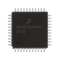
MC9S08AW60CFGE Freescale, MC9S08AW60CFGE Datasheet - Page 73

MC9S08AW60CFGE
Manufacturer Part Number
MC9S08AW60CFGE
Description
Manufacturer
Freescale
Datasheet
1.MC9S08AW60CFGE.pdf
(336 pages)
Specifications of MC9S08AW60CFGE
Cpu Family
HCS08
Device Core Size
8b
Frequency (max)
40MHz
Interface Type
I2C/SCI/SPI
Total Internal Ram Size
2KB
# I/os (max)
34
Number Of Timers - General Purpose
8
Operating Supply Voltage (typ)
3.3/5V
Operating Supply Voltage (max)
5.5V
Operating Supply Voltage (min)
2.7V
On-chip Adc
8-chx10-bit
Instruction Set Architecture
CISC
Operating Temp Range
-40C to 85C
Operating Temperature Classification
Industrial
Mounting
Surface Mount
Pin Count
44
Package Type
LQFP
Program Memory Type
Flash
Program Memory Size
60KB
Lead Free Status / RoHS Status
Compliant
Available stocks
Company
Part Number
Manufacturer
Quantity
Price
Company:
Part Number:
MC9S08AW60CFGE
Manufacturer:
Freescale Semiconductor
Quantity:
10 000
Company:
Part Number:
MC9S08AW60CFGER
Manufacturer:
Freescale Semiconductor
Quantity:
10 000
- Current page: 73 of 336
- Download datasheet (7Mb)
5.9.3
This register contains a single write-only control bit. A serial background command such as
WRITE_BYTE must be used to write to SBDFR. Attempts to write this register from a user program are
ignored. Reads always return 0x00.
Freescale Semiconductor
Reset
BDFR
Field
Field
ILAD
LVD
ICG
3
2
1
0
W
R
1
BDFR is writable only through serial background debug commands, not from user programs.
System Background Debug Force Reset Register (SBDFR)
Illegal Address — Reset was caused by an attempt to access a designated illegal address.
0 Reset not caused by an illegal address access.
1 Reset caused by an illegal address access.
Illegal address areas in the MC9S08AC16 are:
0x0470 - 0x17FF
0x1860 - 0xBFFF — Gap from end of high page registers to start of Flash memory
Unused and reserved locations in register areas are not considered illegal addresses and do not trigger illegal
address resets.
Internal Clock Generation Module Reset — Reset was caused by an ICG module reset.
0 Reset not caused by ICG module.
1 Reset caused by ICG module.
Low Voltage Detect — If the LVDRE and LVDSE bits are set and the supply drops below the LVD trip voltage,
an LVD reset will occur. This bit is also set by POR.
0 Reset not caused by LVD trip or POR.
1 Reset caused by LVD trip or POR.
Background Debug Force Reset — A serial background command such as WRITE_BYTE may be used to
allow an external debug host to force a target system reset. Writing logic 1 to this bit forces an MCU reset. This
bit cannot be written from a user program.
0
0
7
Figure 5-4. System Background Debug Force Reset Register (SBDFR)
= Unimplemented or Reserved
— Gap from end of RAM to start of high page registers
Table 5-4. SRS Register Field Descriptions (continued)
0
0
6
Table 5-5. SBDFR Register Field Descriptions
MC9S08AC16 Series Data Sheet, Rev. 8
0
0
5
0
0
4
Description
Description
Chapter 5 Resets, Interrupts, and System Configuration
3
0
0
0
0
2
0
0
1
BDFR
0
0
0
1
73
Related parts for MC9S08AW60CFGE
Image
Part Number
Description
Manufacturer
Datasheet
Request
R

Part Number:
Description:
TOWER ELEVATOR BOARDS HARDWARE
Manufacturer:
Freescale Semiconductor
Datasheet:

Part Number:
Description:
TOWER SERIAL I/O HARDWARE
Manufacturer:
Freescale Semiconductor
Datasheet:

Part Number:
Description:
LCD MODULE FOR TWR SYSTEM
Manufacturer:
Freescale Semiconductor
Datasheet:

Part Number:
Description:
DAUGHTER LCD WVGA I.MX51
Manufacturer:
Freescale Semiconductor
Datasheet:

Part Number:
Description:
TOWER SYSTEM BOARD MPC5125
Manufacturer:
Freescale Semiconductor
Datasheet:

Part Number:
Description:
KIT EVALUATION I.MX51
Manufacturer:
Freescale Semiconductor
Datasheet:

Part Number:
Description:
KIT DEVELOPMENT WINCE IMX25
Manufacturer:
Freescale Semiconductor
Datasheet:

Part Number:
Description:
TOWER SYSTEM KIT MPC5125
Manufacturer:
Freescale Semiconductor
Datasheet:

Part Number:
Description:
TOWER SYSTEM BOARD K40X256
Manufacturer:
Freescale Semiconductor
Datasheet:

Part Number:
Description:
TOWER SYSTEM KIT K40X256
Manufacturer:
Freescale Semiconductor
Datasheet:

Part Number:
Description:
Microcontrollers (MCU) MX28 PLATFORM DEV KIT
Manufacturer:
Freescale Semiconductor
Datasheet:

Part Number:
Description:
MCU, MPU & DSP Development Tools IAR KickStart Kit for Kinetis K60
Manufacturer:
Freescale Semiconductor
Datasheet:

Part Number:
Description:
24BIT HDMI MX535/08
Manufacturer:
Freescale Semiconductor
Datasheet:
Part Number:
Description:
Manufacturer:
Freescale Semiconductor, Inc
Datasheet:
Part Number:
Description:
Manufacturer:
Freescale Semiconductor, Inc
Datasheet:


