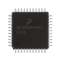
MC9S08AW60CFGE Freescale, MC9S08AW60CFGE Datasheet - Page 85

MC9S08AW60CFGE
Manufacturer Part Number
MC9S08AW60CFGE
Description
Manufacturer
Freescale
Datasheet
1.MC9S08AW60CFGE.pdf
(336 pages)
Specifications of MC9S08AW60CFGE
Cpu Family
HCS08
Device Core Size
8b
Frequency (max)
40MHz
Interface Type
I2C/SCI/SPI
Total Internal Ram Size
2KB
# I/os (max)
34
Number Of Timers - General Purpose
8
Operating Supply Voltage (typ)
3.3/5V
Operating Supply Voltage (max)
5.5V
Operating Supply Voltage (min)
2.7V
On-chip Adc
8-chx10-bit
Instruction Set Architecture
CISC
Operating Temp Range
-40C to 85C
Operating Temperature Classification
Industrial
Mounting
Surface Mount
Pin Count
44
Package Type
LQFP
Program Memory Type
Flash
Program Memory Size
60KB
Lead Free Status / RoHS Status
Compliant
Available stocks
Company
Part Number
Manufacturer
Quantity
Price
Company:
Part Number:
MC9S08AW60CFGE
Manufacturer:
Freescale Semiconductor
Quantity:
10 000
Company:
Part Number:
MC9S08AW60CFGER
Manufacturer:
Freescale Semiconductor
Quantity:
10 000
- Current page: 85 of 336
- Download datasheet (7Mb)
6.3.4
Port D pins are general-purpose I/O pins. Parallel I/O function is controlled by the port D data (PTDD) and
data direction (PTDDD) registers which are located in page zero register space. The pin control registers,
pullup enable (PTDPE), slew rate control (PTDSE), and drive strength select (PTDDS) are located in the
high page registers. Refer to
general-purpose I/O control and
Port D general-purpose I/O are shared with the ADC and KBI. When any of these shared functions is
enabled, the direction, input or output, is controlled by the shared function and not by the data direction
register of the parallel I/O port. When a pin is shared with both the ADC and a digital peripheral function,
the ADC has higher priority. For example, in the case that both the ADC and the KBI are configured to
use PTD7 then the pin is controlled by the ADC module.
Refer to
external clock inputs.
Refer to
port D pins as analog inputs.
Refer to
keyboard inputs.
6.3.5
Port E pins are general-purpose I/O pins. Parallel I/O function is controlled by the port E data (PTED) and
data direction (PTEDD) registers which are located in page zero register space. The pin control registers,
pullup enable (PTEPE), slew rate control (PTESE), and drive strength select (PTEDS) are located in the
high page registers. Refer to
general-purpose I/O control and
Port E general-purpose I/O is shared with SCI1, SPI, and TPM1 timer channels. When any of these shared
functions is enabled, the direction, input or output, is controlled by the shared function and not by the data
direction register of the parallel I/O port. Also, for pins which are configured as outputs by the shared
function, the output data is controlled by the shared function and not by the port data register.
Freescale Semiconductor
Port E
Port D
Chapter 10, “Timer/PWM
Chapter 14, “Analog-to-Digital Converter
Chapter 9, “Keyboard Interrupt
Port D
Port E
MCU Pin:
MCU Pin:
SPSCK1
PTE7/
Bit 7
Section 6.4, “Parallel I/O
Section 6.4, “Parallel I/O
Bit 7
R
Section 6.5, “Pin
Section 6.5, “Pin
MOSI1
PTE6/
MC9S08AC16 Series Data Sheet, Rev. 8
(S08TPMV3)” for more information about using port D pins as TPM
6
Figure 6-5. Port D Pin Names
Figure 6-6. Port E Pin Names
R
6
(S08KBIV1)” for more information about using port D pins as
MISO1
PTE5/
5
R
5
Control” for more information about pin control.
Control” for more information about pin control.
(S08ADC10V1)” for more information about using
Control” for more information about
PTE4/
Control” for more information about
SS1
4
R
4
TPM1CH1
AD1P11/
PTD3/
KBIP6
PTE3/
3
3
AD1P10/
TPM1CH0
PTD2/
KBIP5
PTE2/
2
2
Chapter 6 Parallel Input/Output
AD1P9
PTD1/
1
PTE1/
RxD1
1
AD1P8
PTD0/
Bit 0
PTE0/
TxD1
Bit 0
85
Related parts for MC9S08AW60CFGE
Image
Part Number
Description
Manufacturer
Datasheet
Request
R

Part Number:
Description:
TOWER ELEVATOR BOARDS HARDWARE
Manufacturer:
Freescale Semiconductor
Datasheet:

Part Number:
Description:
TOWER SERIAL I/O HARDWARE
Manufacturer:
Freescale Semiconductor
Datasheet:

Part Number:
Description:
LCD MODULE FOR TWR SYSTEM
Manufacturer:
Freescale Semiconductor
Datasheet:

Part Number:
Description:
DAUGHTER LCD WVGA I.MX51
Manufacturer:
Freescale Semiconductor
Datasheet:

Part Number:
Description:
TOWER SYSTEM BOARD MPC5125
Manufacturer:
Freescale Semiconductor
Datasheet:

Part Number:
Description:
KIT EVALUATION I.MX51
Manufacturer:
Freescale Semiconductor
Datasheet:

Part Number:
Description:
KIT DEVELOPMENT WINCE IMX25
Manufacturer:
Freescale Semiconductor
Datasheet:

Part Number:
Description:
TOWER SYSTEM KIT MPC5125
Manufacturer:
Freescale Semiconductor
Datasheet:

Part Number:
Description:
TOWER SYSTEM BOARD K40X256
Manufacturer:
Freescale Semiconductor
Datasheet:

Part Number:
Description:
TOWER SYSTEM KIT K40X256
Manufacturer:
Freescale Semiconductor
Datasheet:

Part Number:
Description:
Microcontrollers (MCU) MX28 PLATFORM DEV KIT
Manufacturer:
Freescale Semiconductor
Datasheet:

Part Number:
Description:
MCU, MPU & DSP Development Tools IAR KickStart Kit for Kinetis K60
Manufacturer:
Freescale Semiconductor
Datasheet:

Part Number:
Description:
24BIT HDMI MX535/08
Manufacturer:
Freescale Semiconductor
Datasheet:
Part Number:
Description:
Manufacturer:
Freescale Semiconductor, Inc
Datasheet:
Part Number:
Description:
Manufacturer:
Freescale Semiconductor, Inc
Datasheet:


