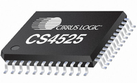
CS4525-CNZR Cirrus Logic Inc, CS4525-CNZR Datasheet - Page 65

CS4525-CNZR
Manufacturer Part Number
CS4525-CNZR
Description
IC PWM Controller+power Stage
Manufacturer
Cirrus Logic Inc
Series
Popguard®r
Type
Class Dr
Datasheet
1.CS4525-CNZ.pdf
(98 pages)
Specifications of CS4525-CNZR
Output Type
2-Channel (Stereo) or 4-Channel (Quad)
Max Output Power X Channels @ Load
30W x 1 @ 4 Ohm; 15W x 2 @ 8 Ohm
Voltage - Supply
8 V ~ 18 V
Features
ADC, Depop, I²C, I²S, Mute, PWM, Short-Circuit and Thermal Protection, Volume Control
Mounting Type
Surface Mount
Package / Case
48-QFN
Lead Free Status / RoHS Status
Lead free / RoHS Compliant
For Use With
598-1586 - REFERENCE BOARD FOR CS4525 PWM
Lead Free Status / RoHS Status
Lead free / RoHS Compliant
Available stocks
Company
Part Number
Manufacturer
Quantity
Price
Part Number:
CS4525-CNZR
Manufacturer:
CIRRUSLOGICINC
Quantity:
20 000
DS726PP3
7. PCB LAYOUT CONSIDERATIONS
7.1
7.2
7.3
Receive acknowledge bit.
Receive byte, contents of selected register.
Send acknowledge bit.
Send stop condition. (Optional.)
Power Supply, Grounding
The CS4525 requires careful attention to power supply and grounding arrangements if its potential perfor-
mance is to be realized. Extensive use of power and ground planes, ground plane fill in unused areas and
surface mount decoupling capacitors are recommended. Decoupling capacitors should be as close to the
pins of the CS4525 as possible. The lowest value ceramic capacitor should be closest to the pin and should
be mounted on the same side of the board as the CS4525 to minimize inductance effects. All signals, es-
pecially clocks, should be kept away from the FILT+ and VQ pins in order to avoid unwanted coupling into
the modulators. The FILT+ and VQ decoupling capacitors, particularly the 0.1 µF, must be positioned to
minimize the electrical path from FILT+ and AGND. The CRD4525 reference design demonstrates the op-
timum layout and power supply arrangements.
Output Filter Layout
The CS4525 also requires careful attention to the layout of the output filter. This will ensure optimum device
performance and EMI standards compliance. The CRD4525 customer reference designs incorporate many
techniques and practices that should be followed in any design using this device and should be referred to
as a guide during the PCB design process. The output components should be placed as close as possible
to the device with the following priority listed from the CS4525 outward:
Avoid any breaks in the ground and power planes beneath high-frequency switching signals. Parasitic in-
ductances should be reduced by the use of multiple smaller vias instead of a single large via when connect-
ing a output filter and power supply bypass capacitors to a ground or power plane. In addition to improving
the thermal performance of the design, filling all unused areas with copper will help reduce both EMI emis-
sions and coupling between adjacent signals. Finally, 150 pF capacitors should be placed directly across
the speaker outputs to shunt remaining high frequency energy prior to the output cables. Any proposed lay-
out should be directly compared to the CRD4525 customer reference designs before manufacture.
QFN Thermal Pad
The underside of the QFN package reveals a large metal pad that serves as a thermal relief to provide for
maximum heat dissipation. This pad must mate with an equally dimensioned copper pad on the PCB and
must be electrically connected to ground. A series of thermal vias should be used to connect this copper
pad to one or more larger ground planes on other PCB layers. The CRD4525 reference design demon-
strates the optimum thermal pad and via configuration.
1. The small value VP bypass capacitors must be placed on the same layer as the CS4525 immediately
2. Following the small value VP bypass capacitors, the RC snubber circuits must be placed on the same
3. The Schottky protection diodes must be placed on the same layer as the CS4525 adjacent to and
4. The LC output filters must be placed on the same layer as the CS4525 adjacent to and immediately
adjacent to the each of the device’s VP pins.
layer as the CS4525 and as close to the device's output pins as possible.
immediately following the RC snubber components.
following the Schottky protection diodes, keeping the trace length as short as possible to reduce
radiated EMI.
CS4525
65


