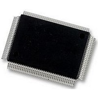
DP83865DVH National Semiconductor, DP83865DVH Datasheet - Page 67

DP83865DVH
Manufacturer Part Number
DP83865DVH
Description
10/100/1000BASE-T TRANSCEIVER, SMD
Manufacturer
National Semiconductor
Specifications of DP83865DVH
Data Rate
1000Mbps
No. Of Ports
1
Ethernet Type
IEEE 802.3u, IEEE 802.3z
Supply Current
430µA
Supply Voltage Range
2.375V To 2.625V, 3.135V To 3.465V
Operating Temperature Range
0°C To +70°C
Interface Type
GMII, MII, RGMII
Rohs Compliant
Yes
Leaded Process Compatible
No
Peak Reflow Compatible (260 C)
No
Lead Free Status / RoHS Status
Lead free / RoHS Compliant
Available stocks
Company
Part Number
Manufacturer
Quantity
Price
Company:
Part Number:
DP83865DVH
Manufacturer:
Texas Instruments
Quantity:
10 000
Company:
Part Number:
DP83865DVH/NOPB
Manufacturer:
NXP
Quantity:
1 000
Company:
Part Number:
DP83865DVH/NOPB
Manufacturer:
Texas Instruments
Quantity:
10 000
5.0 Design Guide
5.8 RJ-45 Connections
The magnetics isolates local circuitry from other equipment
that Ethernet connects to. The IEEE isolation test places
stress on the isolated side to test the dielectic strength of
the isolation. The center tap of the isolated winding has a
"Bob Smith" termination through a 75
pF cap to chassis ground.
should have voltage tolerance of 3 kV (Figure 18).
To pass EMI compliance tests, there are a few helpful rec-
ommendations to follow.
— The RJ-45 is recommended to have metal shielding that
— The isolated side should have the chassis ground "is-
— The MDI pairs are suggested to be routed close together
5.10 Unused Pins and Reserved Pins
Unused CMOS input pins should not be left floating. Float-
ing inputs could have intermediate voltages halfway
between VCC and ground and, as a consequence, turning
on both the NMOS and the PMOS transistors resulting in
high DC current. Floating inputs could also cause oscilla-
tions. Therefore unused inputs should be tied high or low.
In theory CMOS inputs can be directly tied to VCC or GND.
connects to chassis ground to reduce EMI emission.
land" placed. The MDI pairs are placed above a contin-
uous chassis ground plane.
in parallel to reduce EMI emission and common mode
noise (Figure 19).
Figure 19. Differential signal pair
Strap Low
LED active high
Did not maintain parallelism
TP
TP
(Continued)
Differential signal pair
The termination capacitor
GND or power plane
Avoid stubs
Figure 20. LED/strapping option examples.
resistor and 1000
V
DDIO
Strap High
LED active low
= 2.5 V
67
— The EMI can be further reduced by placing the traces in
— Generally, it is a good practice not to overlap the circuit
5.9 LED/Strapping Option
When the LED outputs are used to drive LEDs directly, the
active state of each output driver depends on the logic level
sampled by the corresponding strapping input upon power-
up or reset. For example, if a given LED/strapping pin is
resistively pulled low then the corresponding output is con-
figured as an active high LED driver. Conversely, if a given
LED/strapping pin is resistively pulled high then the corre-
sponding output is configured as an active low LED driver.
Figure 20 is an example of a LED/strapping configuration.
Care must be taken when the multi-function LED/strapping
pins are desired to be programmable. Depending on the
strap low or high state, two sets of jumpers could be used
(Figure 20). The left side jumper position is connected for
the high strap option, and the right side position is con-
nected for the low strap option.
The value of all external pull-up and pull-down resistor
should be 2 k in order to make absolutely certain that the
correct voltage level is applied to the pin.
This method has the advantage of minimizing component
count and board space. However, it is safer to pull the
unused input pins high or low through a current limiting
resistor. This resistor will prevent excessive current drawn
at the input pin in case there is a defect in the input struc-
ture shorting either VCC or GND to the input. Another
advantage of the protection resistor is to reduce the possi-
bility of latch-up. To reduce component count and to save
the inner layers and making the outer layers chassis
ground.
ground plane with the chassis ground that creates cou-
pling. Instead, make chassis ground an isolated island
and make a void between the chassis and circuit ground.
Place two or three 1206 pads across the chassis and cir-
cuit ground void. This will help when experimentally
choosing the appropriate components to pass EMI emis-
sion test.
Header for
jumpers
Programmable
strap high or low
Hi
Hi
V
DDIO
= 2.5 V
Lo
Lo
To LED_pin
www.national.com


