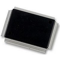
DP83865DVH National Semiconductor, DP83865DVH Datasheet - Page 13

DP83865DVH
Manufacturer Part Number
DP83865DVH
Description
10/100/1000BASE-T TRANSCEIVER, SMD
Manufacturer
National Semiconductor
Specifications of DP83865DVH
Data Rate
1000Mbps
No. Of Ports
1
Ethernet Type
IEEE 802.3u, IEEE 802.3z
Supply Current
430µA
Supply Voltage Range
2.375V To 2.625V, 3.135V To 3.465V
Operating Temperature Range
0°C To +70°C
Interface Type
GMII, MII, RGMII
Rohs Compliant
Yes
Leaded Process Compatible
No
Peak Reflow Compatible (260 C)
No
Lead Free Status / RoHS Status
Lead free / RoHS Compliant
Available stocks
Company
Part Number
Manufacturer
Quantity
Price
Company:
Part Number:
DP83865DVH
Manufacturer:
Texas Instruments
Quantity:
10 000
Company:
Part Number:
DP83865DVH/NOPB
Manufacturer:
NXP
Quantity:
1 000
Company:
Part Number:
DP83865DVH/NOPB
Manufacturer:
Texas Instruments
Quantity:
10 000
1.0 Pin Description
Pin #
23
24
25
26
27
28
29
30
31
32
33
34
35
36
37
38
39
40
41
42
43
44
RESERVED
TCK
CORE_VDD
VSS
TMS
TDO
IO_VDD
VSS
TDI
TRST
RESET
VDD_SEL_STRAP
CORE_VDD
VSS
IO_VDD
VSS
COL
CRS/RGMII_SEL0
RX_ER/RXDV_ER
IO_VDD
VSS
RX_DV/RCK
Data Sheet Pin Name
(Continued)
Table 1.
13
Reserved Reserved: Leave floating.
Ground Ground: Connect to common ground plane.
Ground Ground: Connect to common ground plane.
Ground Ground: Connect to common ground plane.
Ground Ground: Connect to common ground plane.
Ground Ground: Connect to common ground plane.
Output
Output
Output
Output
Output
Power
Power
Power
Power
Power
Strap
Type
Input
Input
Input
Input
Input
JTAG Test Clock: This pin should be left float-
ing if not used.
Core VDD: (Digital) Connect to 1.8V.
JTAG Test Mode Select: This pin should be left
floating if not used.
JTAG Test Data Output: This pin should be left
floating if not used.
I/O VDD: (Digital) Connect to 2.5V or 3.3V. The
VDD_SEL pin must be tied accordingly.
JTAG Test Data Input: This pin should be left
floating if not used.
JTAG Test Reset: This pin should be pulled
down through a 2k resistor if not used.
Reset: Connect to board reset signal.
I/O VDD Select: Pull high to select 3.3V or low
to select 2.5V. The pin must be connected direct-
ly to power or ground (no pull-up/down resistor!).
Core VDD: (Digital) Connect to 1.8V.
I/O VDD: (Digital) Connect to 2.5V or 3.3V. The
VDD_SEL pin must be tied accordingly.
Collision: Connect to MAC chip through a single
50
driving 35 pF load and is not intended to drive
connectors, cables, backplanes or multiple trac-
es. This applies if the part is in 100 Mbps mode
or 1000 Mbps mode.
Carrier Sense: Connect to MAC chip through a
single 50 impedance trace. This output is ca-
pable of driving 35 pf load and is not intended to
drive connectors, cables, backplanes or multiple
traces. This applies if the part is in 100 Mbps
mode or 1000 Mbps mode.
Receive Error: Connect to MAC chip through a
single 50
pable of driving 35 pf load and is not intended to
drive connectors, cables, backplanes or multiple
traces. This applies if the part is in 100 Mbps
mode or 1000 Mbps mode.
I/O VDD: (Digital) Connect to 2.5V or 3.3V. The
VDD_SEL pin must be tied accordingly.
Receive Data Valid: Connect to MAC chip
through a single 50
put is capable of driving 35 pf load and is not in-
tended to drive connectors, cables, backplanes
or multiple traces. This applies if the part is in
100 Mbps mode or 1000 Mbps mode.
impedance trace. This output is capable of
Connection / Comment
impedance trace. This output is ca-
impedance trace. This out-
www.national.com


