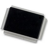
DP83865DVH National Semiconductor, DP83865DVH Datasheet - Page 66

DP83865DVH
Manufacturer Part Number
DP83865DVH
Description
10/100/1000BASE-T TRANSCEIVER, SMD
Manufacturer
National Semiconductor
Specifications of DP83865DVH
Data Rate
1000Mbps
No. Of Ports
1
Ethernet Type
IEEE 802.3u, IEEE 802.3z
Supply Current
430µA
Supply Voltage Range
2.375V To 2.625V, 3.135V To 3.465V
Operating Temperature Range
0°C To +70°C
Interface Type
GMII, MII, RGMII
Rohs Compliant
Yes
Leaded Process Compatible
No
Peak Reflow Compatible (260 C)
No
Lead Free Status / RoHS Status
Lead free / RoHS Compliant
Available stocks
Company
Part Number
Manufacturer
Quantity
Price
Company:
Part Number:
DP83865DVH
Manufacturer:
Texas Instruments
Quantity:
10 000
Company:
Part Number:
DP83865DVH/NOPB
Manufacturer:
NXP
Quantity:
1 000
Company:
Part Number:
DP83865DVH/NOPB
Manufacturer:
Texas Instruments
Quantity:
10 000
www.national.com
5.0 Design Guide
5.6 Layout Notes on MAC Interface
Trace Impedance
All the signal traces of MII and GMII should be impedance
controlled. The trace impedance reference to ground is 50
Ohms. Uncontrolled impedance runs and stubs should be
kept to minimum.
5.6.1 MII, GMII, and RGMII Interfaces
MII and GMII are single ended signals. The output of these
signals are capable of driving 35 pF under worst condi-
tions. However, these outputs are not designed to drive
multiple loads, connectors, backplanes, or cables.
— Place the 49.9
— All the MDI interface traces should have a charateristic
possible to the PHY. Place a 0.01 F decoupling capac-
itor for each channel between 2.5V plane and ground
close to the termination resistor. Place a 0.01 F decou-
pling capacitor for each port at the transformer center
tab.
impedance of 50 Ohms to the GND or 2.5V plane. This
is a strict requirement to minimize return loss.
Figure 17. Signal crossing a plane split
GND or power plane
RJ-45
Chassis Ground
A-
B+
B-
C+
C-
D+
D-
A+
1% termination resistors as close as
Do NOT cross plane split
1000 pF
1
2
3
6
4
5
7
8
(Continued)
3 kV
Figure 18. Twisted Pair/Magnetics interface (Channel A)
75
75
50-Ohm controlled impedance with respect to chassis GND
PULSE H-5007
MCT4
MCT1
MX4+
MX4-
TD4+
TCT4
TD4-
50-Ohm controlled impedance with respect to VDD or GND
66
V
0.01 uF
DDA
Termination Requirement
The purpose of the series termination is to reduce reflec-
tions and to improve the signal quality. The board designer
should evaluate the reflection and signal integrity to deter-
mine the need for the termination in each design. As a gen-
eral rule, if the trace length is less than 1/6 of the
equivalent length of the rise and fall times, the series termi-
nation is not needed. The following is an example of calcu-
lating the signal trace length.
The rise and fall times of GMII are in the order of 500 ps for
RX_CLK, and GTX_CLK. Propagation Delay = 170 ps/inch
on a FR4 board. Equivalent length of rise time = (1/6) Rise
time (ps) / Delay (ps/inch) = (1/6) *(500/ 170) = 0.5 inch.
Thus, series termination is not needed for traces less than
0.5 inch long.
The value of the series termination depends on the driver
output impedance and the characteristic impedance of the
PCB trace. Termination value Rs = characteristic imped-
ance Zo - driver output impedance Ro.
5.7 Twisted Pair Interface
The Twisted Pair Interface consists of four differential
media dependent I/O pairs (MDI_A, MDI_B, MDI_C, and
MDI_D). Each signal is terminated with a 49.9
Figure 18 shows a typical connection for channel A. The
circuitry of channels A, B, C, and D are identical. The MDI
signals are directly connect to 1:1 magnetics. To optimize
the performance, National specifies the key parameters for
the magnetics. Please refer to Section 5.13.2.
The following is a layout guide line for the MDI section.
— Each MDI pair should be placed as close as possible in
— Ideally there should be no crossover or via on the signal
Circuit Ground
= 2.5 V
parallel to minimmize EMI and crosstalk. Each member
of a pair should be matched in length to prevent mis-
match in delay that would cause common mode noise.
paths.
V
DDA
= 2.5 V
0.01 uF
49.9
49.9
MDI_A+
MDI_A-
DP83865
resistor.


