FSBB15CH60C Fairchild Semiconductor, FSBB15CH60C Datasheet - Page 6
FSBB15CH60C
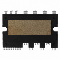
Manufacturer Part Number
FSBB15CH60C
Description
IC POWER MOD SPM 600V SPM27CC
Manufacturer
Fairchild Semiconductor
Series
SPM™r
Type
IGBTr
Specifications of FSBB15CH60C
Configuration
3 Phase
Current
15A
Voltage
600V
Voltage - Isolation
2500Vrms
Package / Case
SPM27CC
Transistor Polarity
N Channel
Dc Collector Current
15A
Collector Emitter Voltage Vces
2V
Power Dissipation Pd
55W
Collector Emitter Voltage V(br)ceo
600V
Operating Temperature Range
-40°C To
Operating Temperature (max)
150C
Operating Temperature (min)
-40C
Pin Count
27
Mounting
Through Hole
Case Length
44mm
Case Height
5.5mm
Screening Level
Automotive
Lead Free Status / RoHS Status
Lead free / RoHS Compliant
Available stocks
Company
Part Number
Manufacturer
Quantity
Price
Company:

Part Number:
FSBB15CH60C
Manufacturer:
CYPRESS
Quantity:
5 610
Part Number:
FSBB15CH60C
Manufacturer:
FSC/ON可看货
Quantity:
20 000


that enables the ground referenced PWM signal to be sent directly to the Mini DIP SPM’s assigned high side
IGBT gate circuit. This level shift function enables opto-coupler-less interface, making it possible to design a
very simple system. In addition a built-in under-voltage lockout (UVLO) protection function interrupts IGBT
operation under control supply under-voltage conditions. Because the bootstrap charge-pump circuit
interconnects to the low-side VCC bias internal to the Mini DIP SPM, the high-side gate drive power can be
obtained from a single 15V control supply referenced to control ground. It is not necessary to have three
isolated voltage sources for the high-side IGBT gate drive required in inverter systems that use conventional
power modules. Mini DIP SPM V4 incorporates built in bootstrap diodes which characteristics are fast
reverse recovery including bootstrap resistance characteristics, about 15 ohm.
fine process technology. Input control logic change from the conventional low active to high active permits
direct interface to 3.3V micro-controllers or DSPs. This provides low circuit current, increased noise immunity
and good performance stability against temperature variation.
dissipation characteristics of a package are critical in determining the Mini DIP SPM performance. A trade-
off exists between heat dissipation characteristics and isolation characteristics. The key to a good package
technology lies in the implementation of outstanding heat dissipation
the isolation rating.
characteristics is attached directly to the lead frame. For expansion to a targeted power rating of 20A and
30A in this same physical package size, DBC (Direct Bonding Copper) technology was applied. In addition,
for optimization of cost to performance up to a power rating of 10A, full molded type technology was applied.
This made it possible to achieve optimum trade-off characteristics while maintaining cost-effectiveness.
lead frame structure was bent to secure the required electrical spacing. In DBC package, the lead frame and
the DBC substrate are directly soldered into the Mini DIP SPM lead frame.
spacing safety regulations required in inverter systems. In Mini DIP SPM, 3.1mm clearance and 4mm
creepage were secured in all areas where high voltage is applied. Exceptionally, 2.65mm clearance and
3.7mm creepage were secured in full molded type package. In addition, the Cu frame pattern and wire
connection have been optimized with the aid of computer simulation for less parasitic inductance, which is
favorable to the suppression of voltage surge at high frequency switching operation.
2008-03-03
Package Technology
Inverter System Technology
Recent progress in the HVIC technology includes chip downsizing through the introduction of wafer
Since heat dissipation is an important factor limiting the power module’s current capability, the heat
In Mini DIP SPM, a technology was developed in which bare ceramic with good heat dissipation
Figure 1.1 shows the cross sections of the Mini DIP SPM V4 package. In full molded packages, the
The Mini DIP SPM package is designed to satisfy the basic UL, IEC and etc. clearance and creepage
V4 Mini DIP SPM Application Note (2008-03-03)
6
FAIRCHILD SEMICONDUCTOR - Smart Power Module
characteristics
without compromising
Related parts for FSBB15CH60C
Image
Part Number
Description
Manufacturer
Datasheet
Request
R

Part Number:
Description:
Fairchild Semiconductor [IGBT MODULE]
Manufacturer:
Fairchild Semiconductor
Datasheet:

Part Number:
Description:
Discrete Semiconductor Modules
Manufacturer:
Fairchild Semiconductor
Part Number:
Description:
Discrete Semiconductor Modules
Manufacturer:
Fairchild Semiconductor
Part Number:
Description:
This N-Channel MOSFET is produced using Fairchild Semiconductor’s advanced Power Trench® process
Manufacturer:
Fairchild Semiconductor
Datasheet:
Part Number:
Description:
This N-Channel MOSFET is produced using Fairchild Semiconductor’s advanced Power Trench® process
Manufacturer:
Fairchild Semiconductor
Datasheet:
Part Number:
Description:
This N-Channel MOSFET is produced using Fairchild Semiconductor’s advanced PowerTrench® process
Manufacturer:
Fairchild Semiconductor
Datasheet:
Part Number:
Description:
This N-Channel MOSFET is produced using Fairchild Semiconductor’s advanced PowerTrench® process
Manufacturer:
Fairchild Semiconductor
Datasheet:
Part Number:
Description:
This N-Channel MOSFET is produced using Fairchild Semiconductor’s advanced Power Trench® process
Manufacturer:
Fairchild Semiconductor
Datasheet:
Part Number:
Description:
This N-Channel logic Level MOSFETs are produced using Fairchild Semiconductor‘s advanced Power Trench® process that has been special tailored to minimize the on-state resistance and yet maintain superior switching performance
Manufacturer:
Fairchild Semiconductor
Datasheet:
Part Number:
Description:
This N-Channel MOSFET is produced using Fairchild Semiconductor’s advanced Power Trench® process
Manufacturer:
Fairchild Semiconductor
Datasheet:
Part Number:
Description:
This N-Channel SyncFET™ is produced using Fairchild Semiconductor’s advanced PowerTrench® process
Manufacturer:
Fairchild Semiconductor
Datasheet:
Part Number:
Description:
This N-Channel SyncFET™ is produced using Fairchild Semiconductor’s advanced PowerTrench® process
Manufacturer:
Fairchild Semiconductor
Datasheet:
Part Number:
Description:
This N-Channel SyncFET™ is produced using Fairchild Semiconductor’s advanced PowerTrench® process
Manufacturer:
Fairchild Semiconductor
Datasheet:
Part Number:
Description:
This N-Channel logic Level MOSFETs are produced using Fairchild Semiconductor‘s advanced Power Trench® process that has been special tailored to minimize the on-state resistance and yet maintain superior switching performance
Manufacturer:
Fairchild Semiconductor
Datasheet:
Part Number:
Description:
This N-Channel MOSFET is produced using Fairchild Semiconductor’s advanced Power Trench® process that has been especially tailored to minimize the on-state resistance and yet maintain superior switching performance
Manufacturer:
Fairchild Semiconductor
Datasheet: