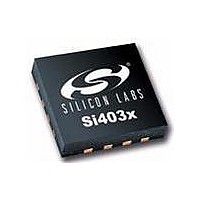
SI4031-B1-FM Silicon Laboratories Inc, SI4031-B1-FM Datasheet - Page 56

SI4031-B1-FM
Manufacturer Part Number
SI4031-B1-FM
Description
IC TX 240-930MHZ -8-13DB 20VQFN
Manufacturer
Silicon Laboratories Inc
Type
ISM Transmitterr
Datasheet
1.SI4031-B1-FMR.pdf
(58 pages)
Specifications of SI4031-B1-FM
Package / Case
20-VQFN
Frequency
240MHz ~ 930MHz
Applications
General Purpose
Modulation Or Protocol
FSK, GFSK, OOK
Data Rate - Maximum
256 kbps
Power - Output
13dBm
Current - Transmitting
30mA
Data Interface
PCB, Surface Mount
Antenna Connector
PCB, Surface Mount
Voltage - Supply
1.8 V ~ 3.6 V
Operating Temperature
-40°C ~ 85°C
Operating Frequency
240 MHz to 930 MHz
Maximum Operating Temperature
+ 85 C
Mounting Style
SMD/SMT
Operating Supply Voltage
1.8 V to 3.6 V
Supply Current
30 mA
Lead Free Status / RoHS Status
Lead free / RoHS Compliant
Features
-
Memory Size
-
Lead Free Status / Rohs Status
Lead free / RoHS Compliant
Available stocks
Company
Part Number
Manufacturer
Quantity
Price
Part Number:
SI4031-B1-FM
Manufacturer:
SILICON LABS/芯科
Quantity:
20 000
Company:
Part Number:
SI4031-B1-FMR
Manufacturer:
INFINEON
Quantity:
12 000
Si4030/31/32-B1
56
Notes: General
Note: Solder Mask Design
Notes: Stencil Design
Notes: Card Assembly
1. All dimensions shown are in millimeters (mm) unless otherwise noted.
2. This land pattern design is based on IPC-7351 guidelines.
1. All metal pads are to be non-solder mask defined (NSMD). Clearance
1. A stainless steel, laser-cut and electro-polished stencil with trapezoidal
2. The stencil thickness should be 0.125 mm (5 mils).
3. The ratio of stencil aperture to land pad size should be 1:1 for the
4. A 2x2 array of 1.10 x 1.10 mm openings on 1.30 mm pitch should be
1. A No-Clean, Type-3 solder paste is recommended.
2. The recommended card reflow profile is per the JEDEC/IPC J-STD-020
between the solder mask and the metal pad is to be 60 µm minimum, all
the way around the pad.
walls should be used to assure good solder paste release.
perimeter pads.
used for the center ground pad.
specification for small body components.
Symbol
C1
C2
X1
X2
Y1
Y2
E
Table 17. PCB Land Pattern Dimensions
Rev 1.1
3.90
3.90
0.20
2.65
0.65
2.65
Min
Millimeters
0.50 REF
Max
4.00
4.00
0.30
2.75
0.75
2.75


