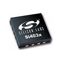
SI4031-B1-FM Silicon Laboratories Inc, SI4031-B1-FM Datasheet - Page 33

SI4031-B1-FM
Manufacturer Part Number
SI4031-B1-FM
Description
IC TX 240-930MHZ -8-13DB 20VQFN
Manufacturer
Silicon Laboratories Inc
Type
ISM Transmitterr
Datasheet
1.SI4031-B1-FMR.pdf
(58 pages)
Specifications of SI4031-B1-FM
Package / Case
20-VQFN
Frequency
240MHz ~ 930MHz
Applications
General Purpose
Modulation Or Protocol
FSK, GFSK, OOK
Data Rate - Maximum
256 kbps
Power - Output
13dBm
Current - Transmitting
30mA
Data Interface
PCB, Surface Mount
Antenna Connector
PCB, Surface Mount
Voltage - Supply
1.8 V ~ 3.6 V
Operating Temperature
-40°C ~ 85°C
Operating Frequency
240 MHz to 930 MHz
Maximum Operating Temperature
+ 85 C
Mounting Style
SMD/SMT
Operating Supply Voltage
1.8 V to 3.6 V
Supply Current
30 mA
Lead Free Status / RoHS Status
Lead free / RoHS Compliant
Features
-
Memory Size
-
Lead Free Status / Rohs Status
Lead free / RoHS Compliant
Available stocks
Company
Part Number
Manufacturer
Quantity
Price
Part Number:
SI4031-B1-FM
Manufacturer:
SILICON LABS/芯科
Quantity:
20 000
Company:
Part Number:
SI4031-B1-FMR
Manufacturer:
INFINEON
Quantity:
12 000
Si4030/31/32-B1
5.3. Crystal Oscillator
The Si4030/31/32 includes an integrated 30 MHz crystal oscillator with a fast start-up time of less than 600 µs
when a suitable parallel resonant crystal is used. The design is differential with the required crystal load
capacitance integrated on-chip to minimize the number of external components. By default, all that is required off-
chip is the 30 MHz crystal.
The crystal load capacitance can be digitally programmed to accommodate crystals with various load capacitance
requirements and to adjust the frequency of the crystal oscillator. The tuning of the crystal load capacitance is
programmed through the xlc[6:0] field of "Register 09h. 30 MHz Crystal Oscillator Load Capacitance." The total
internal capacitance is 12.5 pF and is adjustable in approximately 127 steps (97fF/step). The xtalshift bit is a
coarse shift in frequency but is not binary with xlc[6:0].
The crystal frequency adjustment can be used to compensate for crystal production tolerances. Utilizing the on-
chip temperature sensor and suitable control software, the temperature dependency of the crystal can be
canceled.
The typical value of the total on-chip capacitance Cint can be calculated as follows:
Cint = 1.8 pF + 0.085 pF x xlc[6:0] + 3.7 pF x xtalshift
Note that the coarse shift bit xtalshift is not binary with xlc[6:0]. The total load capacitance Cload seen by the crystal
can be calculated by adding the sum of all external parasitic PCB capacitances Cext to Cint. If the maximum value
of Cint (16.3 pF) is not sufficient, an external capacitor can be added for exact tuning. Additional information on
calculating Cext and crystal selection guidelines is provided in “AN417: Si4x3x Family Crystal Oscillator.”.
The crystal oscillator frequency is divided down internally and may be output to the microcontroller through one of
the GPIO pins for use as the System Clock. In this fashion, only one crystal oscillator is required for the entire
system and the BOM cost is reduced. The available clock frequencies and GPIO configuration are discussed
further in "7.2. Microcontroller Clock" on page 40.
The Si4030/31/32 may also be driven with an external 30 MHz clock signal through the XOUT pin. When driving
with an external reference or using a TCXO, the XTAL load capacitance register should be set to 0.
Add R/W Function/Description
D7
D6
D5
D4
D3
D2
D1
D0
POR Def.
09
R/W
Crystal Oscillator Load
xtalshift
xlc[6]
xlc[5]
xlc[4]
xlc[3]
xlc[2]
xlc[1]
xlc[0]
40h
Capacitance
5.4. Regulators
There are a total of four regulators integrated onto the Si4030/31/32. With the exception of the digital regulator, all
regulators are designed to operate with only internal decoupling. The digital regulator requires an external 1 µF
decoupling capacitor. All regulators are designed to operate with an input supply voltage from +1.8 to +3.6 V. The
output stage of the of PA is not connected internally to a regulator and is connected directly to the battery voltage.
A supply voltage should only be connected to the VDD pins. No voltage should be forced on the digital regulator
output.
Rev 1.1
33


