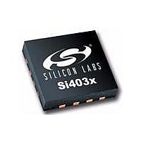
SI4031-B1-FM Silicon Laboratories Inc, SI4031-B1-FM Datasheet - Page 28

SI4031-B1-FM
Manufacturer Part Number
SI4031-B1-FM
Description
IC TX 240-930MHZ -8-13DB 20VQFN
Manufacturer
Silicon Laboratories Inc
Type
ISM Transmitterr
Datasheet
1.SI4031-B1-FMR.pdf
(58 pages)
Specifications of SI4031-B1-FM
Package / Case
20-VQFN
Frequency
240MHz ~ 930MHz
Applications
General Purpose
Modulation Or Protocol
FSK, GFSK, OOK
Data Rate - Maximum
256 kbps
Power - Output
13dBm
Current - Transmitting
30mA
Data Interface
PCB, Surface Mount
Antenna Connector
PCB, Surface Mount
Voltage - Supply
1.8 V ~ 3.6 V
Operating Temperature
-40°C ~ 85°C
Operating Frequency
240 MHz to 930 MHz
Maximum Operating Temperature
+ 85 C
Mounting Style
SMD/SMT
Operating Supply Voltage
1.8 V to 3.6 V
Supply Current
30 mA
Lead Free Status / RoHS Status
Lead free / RoHS Compliant
Features
-
Memory Size
-
Lead Free Status / Rohs Status
Lead free / RoHS Compliant
Available stocks
Company
Part Number
Manufacturer
Quantity
Price
Part Number:
SI4031-B1-FM
Manufacturer:
SILICON LABS/芯科
Quantity:
20 000
Company:
Part Number:
SI4031-B1-FMR
Manufacturer:
INFINEON
Quantity:
12 000
Si4030/31/32-B1
4.2. Modulation Data Source
The Si4030/31/32 may be configured to obtain its modulation data from one of three different sources: FIFO mode,
Direct Mode, and from a PN9 mode. In Direct Mode, the TX modulation data may be obtained from several
different input pins. These options are set through the dtmod[1:0] field in "Register 71h. Modulation Mode Control
2."
4.2.1. FIFO Mode
In FIFO mode, the transmit data is stored in integrated FIFO register memory. The FIFOs are accessed via
"Register 7Fh. FIFO Access," and are most efficiently accessed with burst read/write operation as discussed in
"3.1. Serial Peripheral Interface (SPI)" on page 15.
In TX mode, the data bytes stored in FIFO memory are "packaged" together with other fields and bytes of
information to construct the final transmit packet structure. These other potential fields include the Preamble, Sync
word, Header, CRC checksum, etc. The configuration of the packet structure in TX mode is determined by the
Automatic Packet Handler (if enabled), in conjunction with a variety of Packet Handler Registers (see Table 12 on
page 36). If the Automatic Packet Handler is disabled, the entire desired packet structure should be loaded into
FIFO memory; no other fields (such as Preamble or Sync word are automatically added to the bytes stored in FIFO
memory). For further information on the configuration of the FIFOs for a specific application or packet size, see "6.
Data Handling and Packet Handler" on page 34.
When in FIFO mode, the chip will automatically exit the TX State when either the ipksent or ipkvalid interrupt
occurs. The chip will return to the IDLE mode state programmed in "Register 07h. Operating Mode and Function
Control 1". For example, the chip may be placed into TX mode by setting the txon bit, but with the pllon bit
additionally set. The chip will transmit all of the contents of the FIFO and the ipksent interrupt will occur. When this
interrupt event occurs, the chip will clear the txon bit and return to TUNE mode, as indicated by the set state of the
pllon bit. If no other bits are additionally set in register 07h (besides txon initially), then the chip will return to the
STANDBY state.
28
Add R/W Function/Description
71
dtmod[1:0]
R/W
00
01
10
11
Modulation Mode
Direct Mode using TX Data via GPIO pin (GPIO configuration required)
Direct Mode using TX Data via SDI pin (only when nSEL is high)
FIFO Mode
PN9 (internally generated)
Control 2
trclk[1] trclk[0] dtmod[1] dtmod[0] eninv fd[8] modtyp[1] modtyp[0]
D7
D6
Rev 1.1
D5
Data Source
D4
D3
D2
D1
D0
POR Def.
00h


