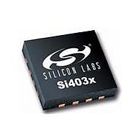
SI4031-B1-FM Silicon Laboratories Inc, SI4031-B1-FM Datasheet - Page 29

SI4031-B1-FM
Manufacturer Part Number
SI4031-B1-FM
Description
IC TX 240-930MHZ -8-13DB 20VQFN
Manufacturer
Silicon Laboratories Inc
Type
ISM Transmitterr
Datasheet
1.SI4031-B1-FMR.pdf
(58 pages)
Specifications of SI4031-B1-FM
Package / Case
20-VQFN
Frequency
240MHz ~ 930MHz
Applications
General Purpose
Modulation Or Protocol
FSK, GFSK, OOK
Data Rate - Maximum
256 kbps
Power - Output
13dBm
Current - Transmitting
30mA
Data Interface
PCB, Surface Mount
Antenna Connector
PCB, Surface Mount
Voltage - Supply
1.8 V ~ 3.6 V
Operating Temperature
-40°C ~ 85°C
Operating Frequency
240 MHz to 930 MHz
Maximum Operating Temperature
+ 85 C
Mounting Style
SMD/SMT
Operating Supply Voltage
1.8 V to 3.6 V
Supply Current
30 mA
Lead Free Status / RoHS Status
Lead free / RoHS Compliant
Features
-
Memory Size
-
Lead Free Status / Rohs Status
Lead free / RoHS Compliant
Available stocks
Company
Part Number
Manufacturer
Quantity
Price
Part Number:
SI4031-B1-FM
Manufacturer:
SILICON LABS/芯科
Quantity:
20 000
Company:
Part Number:
SI4031-B1-FMR
Manufacturer:
INFINEON
Quantity:
12 000
4.2.2. Direct Mode
For legacy systems that perform packet handling within an MCU or other baseband chip, it may not be desirable to
use the FIFO. For this scenario, a Direct Mode is provided which bypasses the FIFOs entirely.
In TX direct mode, the TX modulation data is applied to an input pin of the chip and processed in "real time" (i.e.,
not stored in a register for transmission at a later time). A variety of pins may be configured for use as the TX Data
input function.
Furthermore, an additional pin may be required for a TX Clock output function if GFSK modulation is desired (only
the TX Data input pin is required for FSK). Two options for the source of the TX Data are available in the dtmod[1:0]
field, and various configurations for the source of the TX Data Clock may be selected through the trclk[1:0] field.
The eninv bit in SPI Register 71h will invert the TX Data; this is most likely useful for diagnostic and testing
purposes.
4.2.2.1. Direct Synchronous Mode
In TX direct mode, the chip may be configured for synchronous or asynchronous modes of modulation. In direct
synchronous mode, the RFIC is configured to provide a TX Clock signal as an output to the external device that is
providing the TX Data stream. This TX Clock signal is a square wave with a frequency equal to the programmed
data rate. The external modulation source (e.g., MCU) must accept this TX Clock signal as an input and respond
by providing one bit of TX Data back to the RFIC, synchronous with one edge of the TX Clock signal. In this
fashion, the rate of the TX Data input stream from the external source is controlled by the programmed data rate of
the RFIC; no TX Data bits are made available at the input of the RFIC until requested by another cycle of the TX
Clock signal. The TX Data bits supplied by the external source are transmitted directly in real-time (i.e., not stored
internally for later transmission).
All modulation types (FSK/GFSK/OOK) are valid in TX direct synchronous mode. As will be discussed in the next
section, there are limits on modulation types in TX direct asynchronous mode.
4.2.2.2. Direct Asynchronous Mode
In TX direct asynchronous mode, the RFIC no longer controls the data rate of the TX Data input stream. Instead,
the data rate is controlled only by the external TX Data source; the RFIC simply accepts the data applied to its TX
Data input pin, at whatever rate it is supplied. This means that there is no longer a need for a TX Clock output
signal from the RFIC, as there is no synchronous "handshaking" between the RFIC and the external data source.
The TX Data bits supplied by the external source are transmitted directly in real-time (i.e., not stored internally for
later transmission).
It is not necessary to program the data rate parameter when operating in TX direct asynchronous mode. The chip
still internally samples the incoming TX Data stream to determine when edge transitions occur; however, rather
than sampling the data at a pre-programmed data rate, the chip now internally samples the incoming TX Data
stream at its maximum possible oversampling rate. This allows the chip to accurately determine the timing of the bit
edge transitions without prior knowledge of the data rate. (Of course, it is still necessary to program the desired
peak frequency deviation.)
Only FSK and OOK modulation types are valid in TX Direct Asynchronous Mode; GFSK modulation is not available
in asynchronous mode. This is because the RFIC does not have knowledge of the supplied data rate, and thus
cannot determine the appropriate Gaussian lowpass filter function to apply to the incoming data.
One advantage of this mode that it saves a microcontroller pin because no TX Clock output function is required.
The primary disadvantage of this mode is the increase in occupied spectral bandwidth with FSK (as compared to
GFSK).
trclk[1:0]
00
01
10
11
No TX Clock (only for FSK)
TX Data Clock is available via GPIO (GPIO needs programming accordingly as well)
TX Data Clock is available via SDO pin (only when nSEL is high)
TX Data Clock is available via the nIRQ pin
TX Data Clock Configuration
Rev 1.1
Si4030/31/32-B1
29


