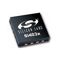
SI4031-B1-FM Silicon Laboratories Inc, SI4031-B1-FM Datasheet - Page 39

SI4031-B1-FM
Manufacturer Part Number
SI4031-B1-FM
Description
IC TX 240-930MHZ -8-13DB 20VQFN
Manufacturer
Silicon Laboratories Inc
Type
ISM Transmitterr
Datasheet
1.SI4031-B1-FMR.pdf
(58 pages)
Specifications of SI4031-B1-FM
Package / Case
20-VQFN
Frequency
240MHz ~ 930MHz
Applications
General Purpose
Modulation Or Protocol
FSK, GFSK, OOK
Data Rate - Maximum
256 kbps
Power - Output
13dBm
Current - Transmitting
30mA
Data Interface
PCB, Surface Mount
Antenna Connector
PCB, Surface Mount
Voltage - Supply
1.8 V ~ 3.6 V
Operating Temperature
-40°C ~ 85°C
Operating Frequency
240 MHz to 930 MHz
Maximum Operating Temperature
+ 85 C
Mounting Style
SMD/SMT
Operating Supply Voltage
1.8 V to 3.6 V
Supply Current
30 mA
Lead Free Status / RoHS Status
Lead free / RoHS Compliant
Features
-
Memory Size
-
Lead Free Status / Rohs Status
Lead free / RoHS Compliant
Available stocks
Company
Part Number
Manufacturer
Quantity
Price
Part Number:
SI4031-B1-FM
Manufacturer:
SILICON LABS/芯科
Quantity:
20 000
Company:
Part Number:
SI4031-B1-FMR
Manufacturer:
INFINEON
Quantity:
12 000
7. Auxiliary Functions
7.1. Smart Reset
The Si4030/31/32 contains an enhanced integrated SMART RESET or POR circuit. The POR circuit contains both
a classic level threshold reset as well as a slope detector POR. This reset circuit was designed to produce a
reliable reset signal under any circumstances. Reset will be initiated if any of the following conditions occur:
The reset will initialize all registers to their default values. The reset signal is also available for output and use by
the microcontroller by using the default setting for GPIO_0. The inverted reset signal is available by default on
GPIO_1.
Initial power on, VDD starts from gnd: reset is active till V
When V
A software reset via “Register 08h. Operating Mode and Function Control 2,” on page 61: reset is active for time
T
V
Release Reset Voltage
Power-On VDD Slope
Low VDD Limit
Software Reset Pulse
Threshold Voltage
Reference Slope
VDD Glitch Reset Pulse
SWRST
DD
glitch when the supply voltage exceeds the following time functioned limit:
DD
Parameter
decreases below V
VDD starts to rise
0.4V
LD
for any reason: reset is active till V
Figure 16. POR Glitch Parameters
TSWRST
Symbol
SVDD
VTSD
VRR
VDD(t)
VLD
TP
k
Table 13. POR Parameters
t=0,
VDD nom.
Also occurs after SDN, and
VLD<VRR is guaranteed
tested VDD slope region
Rev 1.1
initial power on
reset:
Vglitch>=0.4+t*0.2V/ms
Comment
DD
reaches V
showing glitch
actual VDD(t)
Reset
0.4V+t*0.2V/ms
T
P
reset limit:
DD
RR
reaches V
(see table);
Si4030/31/32-B1
t
0.85
0.03
Min
0.7
50
—
—
5
RR
;
Typ
1.3
0.4
0.2
15
—
—
1
Max
1.75
300
470
1.3
40
—
—
V/ms
V/ms
Unit
ms
µs
V
V
V
39


