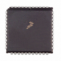
MC68HC711D3CFNE2 Freescale Semiconductor, MC68HC711D3CFNE2 Datasheet - Page 70

MC68HC711D3CFNE2
Manufacturer Part Number
MC68HC711D3CFNE2
Description
IC MCU 8BIT 3MHZ 44-PLCC
Manufacturer
Freescale Semiconductor
Series
HC11r
Specifications of MC68HC711D3CFNE2
Core Processor
HC11
Core Size
8-Bit
Speed
2MHz
Connectivity
SCI, SPI
Peripherals
POR, WDT
Number Of I /o
26
Program Memory Size
4KB (4K x 8)
Program Memory Type
OTP
Ram Size
192 x 8
Voltage - Supply (vcc/vdd)
4.5 V ~ 5.5 V
Oscillator Type
Internal
Operating Temperature
-40°C ~ 85°C
Package / Case
44-PLCC
Lead Free Status / RoHS Status
Lead free / RoHS Compliant
Eeprom Size
-
Data Converters
-
Available stocks
Company
Part Number
Manufacturer
Quantity
Price
Company:
Part Number:
MC68HC711D3CFNE2
Manufacturer:
ALLEGEO
Quantity:
4 492
Company:
Part Number:
MC68HC711D3CFNE2
Manufacturer:
Freescale Semiconductor
Quantity:
10 000
6.7.2 SCI Control Register 1
The SCI control register 1 (SCCR1) provides the control bits that determine word length and select the
method used for the wakeup feature.
R8 — Receive Data Bit 8
T8 — Transmit Data Bit 8
M — Mode Bit
WAKE — Wakeup by Address Mark/Idle Bit
6.7.3 SCI Control Register 2
The SCI control register 2 (SCCR2) provides the control bits that enable or disable individual SCI
functions.
TIE — Transmit Interrupt Enable Bit
TCIE — Transmit Complete Interrupt Enable Bit
RIE — Receiver Interrupt Enable Bit
70
Serial Communications Interface (SCI)
If M bit is set, R8 stores the ninth bit in the receive data character.
If M bit is set, T8 stores ninth bit in transmit data character.
The mode bit selects character format
0 = Start bit, 8 data bits, 1 stop bit
1 = Start bit, 9 data bits, 1 stop bit
0 = Wakeup by IDLE line recognition
1 = Wakeup by address mark (most significant data bit set)
1 = TDRE interrupts disabled
1 = SCI interrupt requested when TDRE status flag is set
0 = TC interrupts disabled
1 = SCI interrupt requested when TC status flag is set
0 = RDRF and OR interrupts disabled
1 = SCI interrupt requested when RDRF flag or the OR status flag is set
Address:
Address:
Reset:
Reset:
Read:
Read:
Write:
Write:
U = Unaffected
$002C
$002D
Bit 7
Bit 7
TIE
R8
U
0
Figure 6-4. SCI Control Register 1 (SCCR1)
Figure 6-5. SCI Control Register 2 (SCCR2)
TCIE
T8
U
6
6
0
MC68HC711D3 Data Sheet, Rev. 2.1
RIE
5
0
0
5
0
ILIE
M
4
0
4
0
WAKE
TE
3
0
3
0
RE
2
0
0
2
0
RWU
1
0
0
1
0
Freescale Semiconductor
Bit 0
Bit 0
SBK
0
0
0


