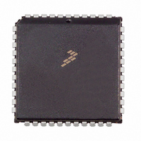
MC68HC711D3CFNE2 Freescale Semiconductor, MC68HC711D3CFNE2 Datasheet - Page 102

MC68HC711D3CFNE2
Manufacturer Part Number
MC68HC711D3CFNE2
Description
IC MCU 8BIT 3MHZ 44-PLCC
Manufacturer
Freescale Semiconductor
Series
HC11r
Specifications of MC68HC711D3CFNE2
Core Processor
HC11
Core Size
8-Bit
Speed
2MHz
Connectivity
SCI, SPI
Peripherals
POR, WDT
Number Of I /o
26
Program Memory Size
4KB (4K x 8)
Program Memory Type
OTP
Ram Size
192 x 8
Voltage - Supply (vcc/vdd)
4.5 V ~ 5.5 V
Oscillator Type
Internal
Operating Temperature
-40°C ~ 85°C
Package / Case
44-PLCC
Lead Free Status / RoHS Status
Lead free / RoHS Compliant
Eeprom Size
-
Data Converters
-
Available stocks
Company
Part Number
Manufacturer
Quantity
Price
Company:
Part Number:
MC68HC711D3CFNE2
Manufacturer:
ALLEGEO
Quantity:
4 492
Company:
Part Number:
MC68HC711D3CFNE2
Manufacturer:
Freescale Semiconductor
Quantity:
10 000
Programmable Timer
8.7.1 Pulse Accumulator Control Register
Four of the pulse accumulator control register (PACTL) bits control an 8-bit pulse accumulator system.
Another bit enables either the OC5 function or the IC4 function, while two other bits select the rate for the
real-time interrupt system.
DDRA7 — Data Direction Control for Port A Bit 7
PAEN — Pulse Accumulator System Enable Bit
PAMOD — Pulse Accumulator Mode Bit
PEDGE — Pulse Accumulator Edge Control Bit
DDRA3 — Data Direction Register for Port A Bit 3
I4/O5 — Input Capture 4/Output Compare 5 Bit
RTR1 and RTR0 — RTI Interrupt Rate Select Bits
102
The pulse accumulator uses port A bit 7 as the PAI input, but the pin can also be used as
general-purpose I/O or as an output compare.
Refer to
This bit has different meanings depending on the state of the PAMOD bit, as shown in
Refer to
Refer to
Refer to
0 = Pulse accumulator disabled
1 = Pulse accumulator enabled
0 = Event counter
1 = Gated time accumulation
Chapter 5 Input/Output (I/O) Ports
Chapter 5 Input/Output (I/O)
8.3 Input
8.5 Real-Time
Address:
Even when port A bit 7 is configured as an output, the pin still drives the
input to the pulse accumulator.
Reset:
Read:
Write:
Figure 8-20. Pulse Accumulator Control Register (PACTL)
Capture.
DDRA7
$0026
Bit 7
PAMOD
0
0
0
1
1
Interrupt.
Table 8-8. Pulse Accumulator Edge Control
PAEN
6
0
PEDGE
0
1
0
1
MC68HC711D3 Data Sheet, Rev. 2.1
PAMOD
PAI falling edge increments the counter.
PAI rising edge increments the counter.
A 0 on PAI inhibits counting.
A 1 on PAI inhibits counting.
Ports.
5
0
for more information.
PEDGE
NOTE
4
0
Action on Clock
DDRA3
3
0
I4/O5
2
0
RTR1
1
0
Freescale Semiconductor
RTR0
Bit 0
0
Table
8-8.


