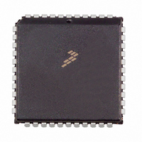
MC68HC711D3CFNE2 Freescale Semiconductor, MC68HC711D3CFNE2 Datasheet - Page 18

MC68HC711D3CFNE2
Manufacturer Part Number
MC68HC711D3CFNE2
Description
IC MCU 8BIT 3MHZ 44-PLCC
Manufacturer
Freescale Semiconductor
Series
HC11r
Specifications of MC68HC711D3CFNE2
Core Processor
HC11
Core Size
8-Bit
Speed
2MHz
Connectivity
SCI, SPI
Peripherals
POR, WDT
Number Of I /o
26
Program Memory Size
4KB (4K x 8)
Program Memory Type
OTP
Ram Size
192 x 8
Voltage - Supply (vcc/vdd)
4.5 V ~ 5.5 V
Oscillator Type
Internal
Operating Temperature
-40°C ~ 85°C
Package / Case
44-PLCC
Lead Free Status / RoHS Status
Lead free / RoHS Compliant
Eeprom Size
-
Data Converters
-
Available stocks
Company
Part Number
Manufacturer
Quantity
Price
Company:
Part Number:
MC68HC711D3CFNE2
Manufacturer:
ALLEGEO
Quantity:
4 492
Company:
Part Number:
MC68HC711D3CFNE2
Manufacturer:
Freescale Semiconductor
Quantity:
10 000
General Description
1.10 Non-Maskable Interrupt/Programming Voltage (XIRQ/V
The XIRQ input provides the capability for asynchronously applying non-maskable interrupts to the MCU
after a power-on reset (POR). During reset, the X bit in the condition code register (CCR) is set masking
any interrupt until enabled by software. This level-sensitive input requires an external pullup resistor to
V
In the programming configuration of the bootstrap mode, this pin is used to supply one-time
programmable read-only memory (OTPROM) programming voltage, V
programming accidents during reset, this pin should be equal to V
XIRQ is active.
1.11 MODA and MODB (MODA/LIR and MODB/V
As reset transitions, these pins are used to latch the part into one of the four central processor unit (CPU)
controlled modes of operation. The LIR output can be used as an aid to debugging once reset is
completed. The open-drain LIR pin goes to an active low during the first E-clock cycle of each instruction
and remains low for the duration of that cycle. The V
(RAM) contents during power down.
1.12 Read/Write (R/W)
This pin performs either of two separate functions, depending on the operating mode.
1.13 Port D Bit 6/Address Strobe (PD6/AS)
This pin performs either of two separate functions, depending on the operating mode.
Refer to
1.14 Input/Output Lines (PA7–PA0, PB7–PB0, PC7–PC0, and PD7–PD0)
In the 44-pin PLCC package, 32 input/output lines are arranged into four 8-bit ports: A, B, C, and D. The
lines of ports B, C, and D are fully bidirectional. Port A has two bidirectional, three input-only, and three
output-only lines in the 44-pin PLCC packaging. In the 40-pin DIP, two of the output-only lines are not
bonded.
Each of these four ports serves a purpose other than input/output (I/O), depending on the operating mode
or peripheral functions selected.
18
DD
•
•
•
•
.
In single-chip and bootstrap modes, R/W functions as input/output port D bit 7. Refer to
In expanded multiplexed and test modes, R/W performs a read/write function. R/W controls the
direction of transfers on the external data bus.
In single-chip and bootstrap modes, the pin functions as input/output port D bit 6.
In the expanded multiplexed and test modes, it provides an address strobe (AS) function. AS is
used to demultiplex the address and data signals at port C.
Input/Output (I/O) Ports
Chapter 2 Operating Modes and Memory
Ports B, C, and two bits of port D are available for I/O functions only in
single-chip and bootstrap modes.
for further information.
MC68HC711D3 Data Sheet, Rev. 2.1
NOTE
for further information.
STBY
input is used to retain random-access memory
DD
STBY
during normal operation unless
PP
)
, to the MCU. To avoid
PP
Freescale Semiconductor
)
Chapter 5


