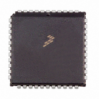
MC68HC711D3CFNE2 Freescale Semiconductor, MC68HC711D3CFNE2 Datasheet - Page 61

MC68HC711D3CFNE2
Manufacturer Part Number
MC68HC711D3CFNE2
Description
IC MCU 8BIT 3MHZ 44-PLCC
Manufacturer
Freescale Semiconductor
Series
HC11r
Specifications of MC68HC711D3CFNE2
Core Processor
HC11
Core Size
8-Bit
Speed
2MHz
Connectivity
SCI, SPI
Peripherals
POR, WDT
Number Of I /o
26
Program Memory Size
4KB (4K x 8)
Program Memory Type
OTP
Ram Size
192 x 8
Voltage - Supply (vcc/vdd)
4.5 V ~ 5.5 V
Oscillator Type
Internal
Operating Temperature
-40°C ~ 85°C
Package / Case
44-PLCC
Lead Free Status / RoHS Status
Lead free / RoHS Compliant
Eeprom Size
-
Data Converters
-
Available stocks
Company
Part Number
Manufacturer
Quantity
Price
Company:
Part Number:
MC68HC711D3CFNE2
Manufacturer:
ALLEGEO
Quantity:
4 492
Company:
Part Number:
MC68HC711D3CFNE2
Manufacturer:
Freescale Semiconductor
Quantity:
10 000
Chapter 5
Input/Output (I/O) Ports
5.1 Introduction
The MC68HC711D3 has four 8-bit input/output (I/O) ports; A, B, C, and D. In the 40-pin version, port A
bits 4 and 6 are not bonded. Port functions are controlled by the particular mode of operation selected, as
shown in
In the single-chip and bootstrap modes, all the ports are configured as parallel input/output (I/O) data
ports. In expanded multiplexed and test modes, ports B, C, and lines D6 (AS) and D7 (R/W) are
configured as a memory expansion bus, with:
The remaining ports are unaffected by mode changes.
5.2 Port A
Port A shares functions with the timer system and has:
Pins PA6 and PA4 are not bonded in the 40-pin dual in-line package (DIP), and their OC output functions
are unavailable, but their software interrupts are available.
Freescale Semiconductor
•
•
•
•
•
•
•
•
•
•
Port B as the high-order address bus
Port C as the multiplexed address and data bus
AS as the demultiplexing signal
R/W as data bus direction control
Ports A and D can be used as general-purpose I/O ports, though each has an alternate function.
Port A bits handle the timer functions.
Port D handles serial peripheral interface (SPI) and serial communications interface (SCI)
functions in addition to its bus direction control functions.
Three input only pins
Three output only pins
Two bidirectional I/O pins
Table 1-1. Port Signal
Alt. Func.:
Address:
And/Or:
Reset:
Read:
Write:
1. This pin is not bonded in the 40-pin version.
$0000
Bit 7
OC1
PA7
Hi-Z
PAI
Figure 5-1. Port A Data Register (PORTA)
PA6
Functions.
OC2
OC1
6
0
(1)
MC68HC711D3 Data Sheet, Rev. 2.1
OC3
OC1
PA5
5
0
PA4
OC4
OC1
4
0
(1)
IC4/OC5
OC1
PA3
Hi-Z
3
PA2
Hi-Z
IC1
—
2
PA1
Hi-Z
IC2
—
1
Bit 0
PA0
Hi-Z
IC3
—
61


