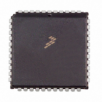
MC68HC711D3CFNE2 Freescale Semiconductor, MC68HC711D3CFNE2 Datasheet - Page 16

MC68HC711D3CFNE2
Manufacturer Part Number
MC68HC711D3CFNE2
Description
IC MCU 8BIT 3MHZ 44-PLCC
Manufacturer
Freescale Semiconductor
Series
HC11r
Specifications of MC68HC711D3CFNE2
Core Processor
HC11
Core Size
8-Bit
Speed
2MHz
Connectivity
SCI, SPI
Peripherals
POR, WDT
Number Of I /o
26
Program Memory Size
4KB (4K x 8)
Program Memory Type
OTP
Ram Size
192 x 8
Voltage - Supply (vcc/vdd)
4.5 V ~ 5.5 V
Oscillator Type
Internal
Operating Temperature
-40°C ~ 85°C
Package / Case
44-PLCC
Lead Free Status / RoHS Status
Lead free / RoHS Compliant
Eeprom Size
-
Data Converters
-
Available stocks
Company
Part Number
Manufacturer
Quantity
Price
Company:
Part Number:
MC68HC711D3CFNE2
Manufacturer:
ALLEGEO
Quantity:
4 492
Company:
Part Number:
MC68HC711D3CFNE2
Manufacturer:
Freescale Semiconductor
Quantity:
10 000
General Description
1.5 Power Supply (V
Power is supplied to the MCU through V
ground (0 V). EV
1.6 Reset (RESET)
An active low bidirectional control signal, RESET, acts as an input to initialize the MCU to a known startup
state. It also acts as an open-drain output to indicate that an internal failure has been detected in either
the clock monitor or computer operating properly (COP) watchdog circuit. In addition, the state of this pin
is one of the factors governing the selection of BOOT mode.
1.7 Crystal Driver and External Clock Input (XTAL and EXTAL)
These two pins provide the interface for either a crystal or a CMOS compatible clock to control the internal
clock generator circuitry. The frequency applied to these pins is four times higher than the desired E-clock
rate. Refer to
1.8 E-Clock Output (E)
E is the output connection for the internally generated E clock. The signal from E is used as a timing
reference. The frequency of the E-clock output is one fourth that of the input frequency at the XTAL and
EXTAL pins. The E clock can be turned off in single-chip mode for greater noise immunity if desired. See
4.3.6 Highest Priority I Interrupt and Miscellaneous Register (HPRIO)
16
Figure 1-5
SS
, available on the 44-pin PLCC and QFP, is an additional ground pin.
for crystal and clock connections.
DD
Figure 1-4. Pin Assignments for 44-Pin QFP
RESET
XIRQ
PC4
PC5
PC6
PC7
PD7
PD6
PD0
PD1
IRQ
, V
SS
MC68HC711D3 Data Sheet, Rev. 2.1
1
2
3
4
5
6
7
8
9
10
, and EV
DD
and V
SS
SS
. V
)
DD
is the power supply (+5 V ±10%) and V
32
31
30
29
28
27
26
25
24
23
for details.
PB0
PB1
PB2
PB3
PB4
PB5
PB6
PB7
NC
PA0
PA1
Freescale Semiconductor
SS
is


