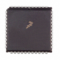
MC68HC711D3CFNE2 Freescale Semiconductor, MC68HC711D3CFNE2 Datasheet - Page 29

MC68HC711D3CFNE2
Manufacturer Part Number
MC68HC711D3CFNE2
Description
IC MCU 8BIT 3MHZ 44-PLCC
Manufacturer
Freescale Semiconductor
Series
HC11r
Specifications of MC68HC711D3CFNE2
Core Processor
HC11
Core Size
8-Bit
Speed
2MHz
Connectivity
SCI, SPI
Peripherals
POR, WDT
Number Of I /o
26
Program Memory Size
4KB (4K x 8)
Program Memory Type
OTP
Ram Size
192 x 8
Voltage - Supply (vcc/vdd)
4.5 V ~ 5.5 V
Oscillator Type
Internal
Operating Temperature
-40°C ~ 85°C
Package / Case
44-PLCC
Lead Free Status / RoHS Status
Lead free / RoHS Compliant
Eeprom Size
-
Data Converters
-
Available stocks
Company
Part Number
Manufacturer
Quantity
Price
Company:
Part Number:
MC68HC711D3CFNE2
Manufacturer:
ALLEGEO
Quantity:
4 492
Company:
Part Number:
MC68HC711D3CFNE2
Manufacturer:
Freescale Semiconductor
Quantity:
10 000
2.3.2 RAM and I/O Mapping Register
The random-access memory (RAM) and input/output (I/O) mapping register (INIT) is a special-purpose
8-bit register that is used during initialization to change the default locations of RAM and control registers
within the MCU memory map. It can be written to only once within the first 64 E-clock cycles after a reset
in normal modes. Thereafter, it becomes a read-only register.
Freescale Semiconductor
$003C
$003D
$003A
$003B
$003E
$003F
Addr.
1. The values of the RBOOT, SMOD, IRVNE, and MDA bits at reset depend on the mode during initialization. Refer to
Table 4-3. Hardware Mode Select
Highest Priority I-Bit Interrupt and
Miscellaneous Register (HPRIO)
Arm/Reset COP Timer Circuitry
RAM and I/O Mapping Register
System Configuration Register
PROM Programming Control
Register Name
Address:
Reset:
Read:
Write:
Register (COPRST)
Register (PPROG)
Figure 2-2. Register and Control Bit Assignments (Sheet 5 of 5)
Test 1 Register
See page 48.
See page 32.
See page 58.
See page 29.
See page 30.
$003D
RAM3
Bit 7
(CONFIG)
0
(TEST)
Figure 2-3. RAM and I/O Mapping Register (INIT)
(INIT)
RAM2
Reset:
Reset:
Reset:
Reset:
Reset:
Reset:
Read:
Read:
Read:
Read:
Read:
Read:
Write:
Write:
Write:
Write:
Write:
Write:
Summary.
6
0
MC68HC711D3 Data Sheet, Rev. 2.1
RBOOT
TILOP
RAM3
Bit 7
MBE
Bit 7
RAM1
0
0
0
0
0
0
5
0
= Unimplemented
SMOD
RAM2
Bit 6
6
0
0
0
0
0
0
0
0
RAM0
4
0
Note 1
RAM1
OCC4
ELAT
MDA
Bit 5
5
0
0
0
0
0
0
REG3
3
0
EXCOL
IRVNE
RAM0
CBYP
Bit 4
R
4
0
0
0
0
0
0
REG2
2
0
= Reserved
EXROW
PSEL3
REG3
DISR
Bit 3
3
0
0
0
0
0
0
0
REG1
1
0
NOCOP
PSEL2
REG2
FCM
Bit 2
U
2
0
0
0
1
0
0
REG0
Bit 0
0
U = Unaffected
ROMON
PSEL1
FCOP
REG1
Bit 1
U
1
0
0
0
0
0
0
Memory Map
PSEL0
REG0
PGM
Bit 0
Bit 0
0
0
1
1
0
0
0
0
29


