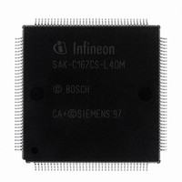
SAK-C167CS-L40M CA+ Infineon Technologies, SAK-C167CS-L40M CA+ Datasheet - Page 68

SAK-C167CS-L40M CA+
Manufacturer Part Number
SAK-C167CS-L40M CA+
Description
IC MCU 16BIT 40MHZ MQFP-144
Manufacturer
Infineon Technologies
Series
C16xxr
Datasheet
1.SAK-C167CS-LM_CA.pdf
(81 pages)
Specifications of SAK-C167CS-L40M CA+
Core Processor
C166
Core Size
16-Bit
Speed
40MHz
Connectivity
CAN, EBI/EMI, SPI, SSC, UART/USART
Peripherals
POR, PWM, WDT
Number Of I /o
111
Program Memory Type
ROMless
Ram Size
11K x 8
Voltage - Supply (vcc/vdd)
4.5 V ~ 5.5 V
Data Converters
A/D 24x10b
Oscillator Type
External
Operating Temperature
-40°C ~ 125°C
Package / Case
144- BSQFP
Data Bus Width
16 bit
Data Ram Size
11 KB
Interface Type
1xUSART, 1xSSC
Maximum Clock Frequency
40 MHz
Number Of Programmable I/os
111
Number Of Timers
9
Operating Supply Voltage
5 V
Maximum Operating Temperature
+ 125 C
Mounting Style
SMD/SMT
Minimum Operating Temperature
- 40 C
On-chip Adc
10 bit, 24 Channel
Packages
PG-MQFP-144
Max Clock Frequency
40.0 MHz
Sram (incl. Cache)
11.0 KByte
Can Nodes
2
A / D Input Lines (incl. Fadc)
24
Program Memory
0.0 KByte
Lead Free Status / RoHS Status
Lead free / RoHS Compliant
Eeprom Size
-
Program Memory Size
-
Lead Free Status / Rohs Status
Details
Other names
K167CSL40MCAZNP
K167CSL40MCAZXP
SAK-C167CS-L40M CA+
SAK-C167CS-L40MCAIN
SAKC167CSL40MCAXT
SP000103490
K167CSL40MCAZXP
SAK-C167CS-L40M CA+
SAK-C167CS-L40MCAIN
SAKC167CSL40MCAXT
SP000103490
Table 17
Parameter
Output delay from CLKOUT falling edge
Valid for: address (MUX on PORT0), write data out
Output delay from CLKOUT edge
Valid for: latched CS, ALE (normal)
Output delay from CLKOUT edge
Valid for: WR, WRL, WRH, WrCS
Output delay from CLKOUT edge
Valid for: RD, RdCS
Input setup time to CLKOUT falling edge
Valid for: read data in
Input hold time after CLKOUT falling edge
Valid for: read data in
Output delay from CLKOUT falling edge
Valid for: address (on PORT1 and/or P4), BHE
Output hold time after CLKOUT falling edge
Valid for: address, BHE
Output hold time after CLKOUT edge
Valid for: write data out
Output delay from CLKOUT falling edge
Valid for: ALE (extended), early CS
Turn off delay after CLKOUT edge
Valid for: write data out
Turn on delay after CLKOUT falling edge
Valid for: write data out
Output hold time after CLKOUT edge
Valid for: early CS
1)
2)
3)
4)
Data Sheet
Read data are latched with the same (internal) clock edge that triggers the address change and the rising edge
of RD. Therefore address changes before the end of RD have no impact on (demultiplexed) read cycles.
If the capacitive load on the respective output pins is limited to 30 pF the maximum output delay
reduced to 8 ns.
Due to comparable propagation delays the address does not change before WR goes high. The minimum
output delay (
Not 100% tested, guaranteed by design and characterization.
tc
External Bus Cycle Timing (Operating Conditions apply)
17min
) is therefore the actual value of
1)
3)
4)
4)
4)
64
tc
12
.
Symbol
tc
tc
tc
tc
tc
tc
tc
tc
tc
tc
tc
tc
tc
10
11
12
13
14
15
16
17
18
19
20
21
22
CC 0
CC -3
CC -4
CC -2
SR 10
SR 0
CC 0
CC -2
CC -1
CC -4
CC –
CC -5
CC -6
min.
Limits
max.
14
6
7
7
–
–
9
8
–
4
7
–
4
C167CS-4R
2)
V2.2, 2001-08
C167CS-L
tc
16
Unit
ns
ns
ns
ns
ns
ns
ns
ns
ns
ns
ns
ns
ns
can be


