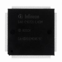
SAK-C167CS-L40M CA+ Infineon Technologies, SAK-C167CS-L40M CA+ Datasheet - Page 13

SAK-C167CS-L40M CA+
Manufacturer Part Number
SAK-C167CS-L40M CA+
Description
IC MCU 16BIT 40MHZ MQFP-144
Manufacturer
Infineon Technologies
Series
C16xxr
Datasheet
1.SAK-C167CS-LM_CA.pdf
(81 pages)
Specifications of SAK-C167CS-L40M CA+
Core Processor
C166
Core Size
16-Bit
Speed
40MHz
Connectivity
CAN, EBI/EMI, SPI, SSC, UART/USART
Peripherals
POR, PWM, WDT
Number Of I /o
111
Program Memory Type
ROMless
Ram Size
11K x 8
Voltage - Supply (vcc/vdd)
4.5 V ~ 5.5 V
Data Converters
A/D 24x10b
Oscillator Type
External
Operating Temperature
-40°C ~ 125°C
Package / Case
144- BSQFP
Data Bus Width
16 bit
Data Ram Size
11 KB
Interface Type
1xUSART, 1xSSC
Maximum Clock Frequency
40 MHz
Number Of Programmable I/os
111
Number Of Timers
9
Operating Supply Voltage
5 V
Maximum Operating Temperature
+ 125 C
Mounting Style
SMD/SMT
Minimum Operating Temperature
- 40 C
On-chip Adc
10 bit, 24 Channel
Packages
PG-MQFP-144
Max Clock Frequency
40.0 MHz
Sram (incl. Cache)
11.0 KByte
Can Nodes
2
A / D Input Lines (incl. Fadc)
24
Program Memory
0.0 KByte
Lead Free Status / RoHS Status
Lead free / RoHS Compliant
Eeprom Size
-
Program Memory Size
-
Lead Free Status / Rohs Status
Details
Other names
K167CSL40MCAZNP
K167CSL40MCAZXP
SAK-C167CS-L40M CA+
SAK-C167CS-L40MCAIN
SAKC167CSL40MCAXT
SP000103490
K167CSL40MCAZXP
SAK-C167CS-L40M CA+
SAK-C167CS-L40MCAIN
SAKC167CSL40MCAXT
SP000103490
Table 2
Symbol Pin
P4
P4.0
P4.1
P4.2
P4.3
P4.4
P4.5
P4.6
P4.7
RD
WR/
WRL
READY 97
Data Sheet
Num.
85
86
87
88
89
90
91
92
95
96
Pin Definitions and Functions (cont’d)
Input
Outp.
IO
O
O
O
O
O
I
O
I
O
O
O
O
I
O
I
O
O
I
Function
Port 4 is an 8-bit bidirectional I/O port. It is bit-wise
programmable for input or output via direction bits. For a pin
configured as input, the output driver is put into high-
impedance state. The Port 4 outputs can be configured as
push/pull or open drain drivers. The input threshold of Port 4
is selectable (TTL or special).
Port 4 can be used to output the segment address lines and
for serial interface lines:
A16
A17
A18
A19
A20
CAN2_RxD CAN 2 Receive Data Input
A21
CAN1_RxD CAN 1 Receive Data Input
A22
CAN1_TxD CAN 1 Transmit Data Output,
CAN2_TxD CAN 2 Transmit Data Output
A23
CAN1_RxD CAN 1 Receive Data Input,
CAN2_TxD CAN 2 Transmit Data Output,
CAN2_RxD CAN 2 Receive Data Input
External Memory Read Strobe. RD is activated for every
external instruction or data read access.
External Memory Write Strobe. In WR-mode this pin is
activated for every external data write access. In WRL-mode
this pin is activated for low byte data write accesses on a
16-bit bus, and for every data write access on an 8-bit bus.
See WRCFG in register SYSCON for mode selection.
Ready Input. When the Ready function is enabled, a high
level at this pin during an external memory access will force
the insertion of memory cycle time waitstates until the pin
returns to a low level.
An internal pullup device will hold this pin high when nothing
is driving it.
Least Significant Segment Address Line
Segment Address Line
Segment Address Line
Segment Address Line
Segment Address Line,
Segment Address Line,
Segment Address Line,
Most Significant Segment Address Line,
9
1)
C167CS-4R
V2.2, 2001-08
C167CS-L


