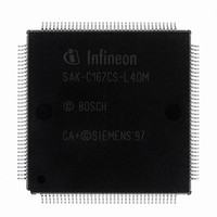
SAK-C167CS-L40M CA+ Infineon Technologies, SAK-C167CS-L40M CA+ Datasheet - Page 21

SAK-C167CS-L40M CA+
Manufacturer Part Number
SAK-C167CS-L40M CA+
Description
IC MCU 16BIT 40MHZ MQFP-144
Manufacturer
Infineon Technologies
Series
C16xxr
Datasheet
1.SAK-C167CS-LM_CA.pdf
(81 pages)
Specifications of SAK-C167CS-L40M CA+
Core Processor
C166
Core Size
16-Bit
Speed
40MHz
Connectivity
CAN, EBI/EMI, SPI, SSC, UART/USART
Peripherals
POR, PWM, WDT
Number Of I /o
111
Program Memory Type
ROMless
Ram Size
11K x 8
Voltage - Supply (vcc/vdd)
4.5 V ~ 5.5 V
Data Converters
A/D 24x10b
Oscillator Type
External
Operating Temperature
-40°C ~ 125°C
Package / Case
144- BSQFP
Data Bus Width
16 bit
Data Ram Size
11 KB
Interface Type
1xUSART, 1xSSC
Maximum Clock Frequency
40 MHz
Number Of Programmable I/os
111
Number Of Timers
9
Operating Supply Voltage
5 V
Maximum Operating Temperature
+ 125 C
Mounting Style
SMD/SMT
Minimum Operating Temperature
- 40 C
On-chip Adc
10 bit, 24 Channel
Packages
PG-MQFP-144
Max Clock Frequency
40.0 MHz
Sram (incl. Cache)
11.0 KByte
Can Nodes
2
A / D Input Lines (incl. Fadc)
24
Program Memory
0.0 KByte
Lead Free Status / RoHS Status
Lead free / RoHS Compliant
Eeprom Size
-
Program Memory Size
-
Lead Free Status / Rohs Status
Details
Other names
K167CSL40MCAZNP
K167CSL40MCAZXP
SAK-C167CS-L40M CA+
SAK-C167CS-L40MCAIN
SAKC167CSL40MCAXT
SP000103490
K167CSL40MCAZXP
SAK-C167CS-L40M CA+
SAK-C167CS-L40MCAIN
SAKC167CSL40MCAXT
SP000103490
Note: When one or both of the on-chip CAN Modules are used with the interface lines
Central Processing Unit (CPU)
The main core of the CPU consists of a 4-stage instruction pipeline, a 16-bit arithmetic
and logic unit (ALU) and dedicated SFRs. Additional hardware has been spent for a
separate multiply and divide unit, a bit-mask generator and a barrel shifter.
Based on these hardware provisions, most of the C167CS’s instructions can be
executed in just one machine cycle which requires 50 ns at 40 MHz CPU clock. For
example, shift and rotate instructions are always processed during one machine cycle
independent of the number of bits to be shifted. All multiple-cycle instructions have been
optimized so that they can be executed very fast as well: branches in 2 cycles, a 16 ×
16 bit multiplication in 5 cycles and a 32-/16-bit division in 10 cycles. Another pipeline
optimization, the so-called ‘Jump Cache’, allows reducing the execution time of
repeatedly performed jumps in a loop from 2 cycles to 1 cycle.
Figure 4
Data Sheet
ROM
assigned to Port 4, the CAN lines override the segment address lines and the
segment address output on Port 4 is therefore limited to 6/4 bits i.e. address lines
A21/A19 … A16. CS lines can be used to increase the total amount of
addressable external memory.
CPU Block Diagram
32
Data Page Ptr.
Exec. Unit
Instr. Reg.
SYSCON
Instr. Ptr.
BUSCON 1
BUSCON 0
BUSCON 2
BUSCON 3
BUSCON 4
STKUN
STKOV
PSW
SP
Pipeline
4-Stage
Barrel - Shifter
Bit-Mask Gen
Code Seg. Ptr.
Mul/Div-HW
Context Ptr.
ADDRSEL 1
ADDRSEL 3
ADDRSEL 4
ADDRSEL 2
ALU
MDH
MDL
CPU
17
(16-bit)
Registers
Purpose
General
R15
R0
16
16
C167CS-4R
V2.2, 2001-08
C167CS-L
Internal
RAM
R15
R0
MCB02147


