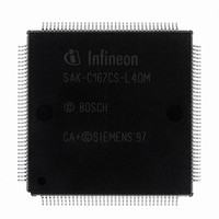
SAK-C167CS-L40M CA+ Infineon Technologies, SAK-C167CS-L40M CA+ Datasheet - Page 60

SAK-C167CS-L40M CA+
Manufacturer Part Number
SAK-C167CS-L40M CA+
Description
IC MCU 16BIT 40MHZ MQFP-144
Manufacturer
Infineon Technologies
Series
C16xxr
Datasheet
1.SAK-C167CS-LM_CA.pdf
(81 pages)
Specifications of SAK-C167CS-L40M CA+
Core Processor
C166
Core Size
16-Bit
Speed
40MHz
Connectivity
CAN, EBI/EMI, SPI, SSC, UART/USART
Peripherals
POR, PWM, WDT
Number Of I /o
111
Program Memory Type
ROMless
Ram Size
11K x 8
Voltage - Supply (vcc/vdd)
4.5 V ~ 5.5 V
Data Converters
A/D 24x10b
Oscillator Type
External
Operating Temperature
-40°C ~ 125°C
Package / Case
144- BSQFP
Data Bus Width
16 bit
Data Ram Size
11 KB
Interface Type
1xUSART, 1xSSC
Maximum Clock Frequency
40 MHz
Number Of Programmable I/os
111
Number Of Timers
9
Operating Supply Voltage
5 V
Maximum Operating Temperature
+ 125 C
Mounting Style
SMD/SMT
Minimum Operating Temperature
- 40 C
On-chip Adc
10 bit, 24 Channel
Packages
PG-MQFP-144
Max Clock Frequency
40.0 MHz
Sram (incl. Cache)
11.0 KByte
Can Nodes
2
A / D Input Lines (incl. Fadc)
24
Program Memory
0.0 KByte
Lead Free Status / RoHS Status
Lead free / RoHS Compliant
Eeprom Size
-
Program Memory Size
-
Lead Free Status / Rohs Status
Details
Other names
K167CSL40MCAZNP
K167CSL40MCAZXP
SAK-C167CS-L40M CA+
SAK-C167CS-L40MCAIN
SAKC167CSL40MCAXT
SP000103490
K167CSL40MCAZXP
SAK-C167CS-L40M CA+
SAK-C167CS-L40MCAIN
SAKC167CSL40MCAXT
SP000103490
P0.15-13 (P0H.7-5). Register RP0H can be loaded from the upper half of register
RSTCON under software control.
Table 11
generation mode.
Table 11
CLKCFG
(RP0H.7-5)
1)
2)
3)
Prescaler Operation
When prescaler operation is configured (CLKCFG = 001
the internal oscillator (input clock signal) by a 2:1 prescaler.
The frequency of
the duration of an individual TCL) is defined by the period of the input clock
The timings listed in the AC Characteristics that refer to TCLs therefore can be
calculated using the period of
Phase Locked Loop
When PLL operation is configured (via CLKCFG) the on-chip phase locked loop is
enabled and provides the CPU clock (see
frequency by the factor F which is selected via the combination of pins P0.15-13 (i.e.
f
clock to the input clock. This synchronization is done smoothly, i.e. the CPU clock
frequency does not change abruptly.
Data Sheet
CPU
1 1 1
1 1 0
1 0 1
1 0 0
0 1 1
0 1 0
0 0 1
0 0 0
The external clock input range refers to a CPU clock range of 10 … 40 MHz.
The maximum frequency depends on the duty cycle of the external clock signal.
In prescaler mode the full CPU clock range cannot be used.
=
f
OSC
associates the combinations of these three bits with the respective clock
× F). With every F’th transition of
CPU Frequency
f
f
f
f
f
f
f
f
f
OSC
OSC
OSC
OSC
OSC
OSC
OSC
OSC
C167CS Clock Generation Modes
CPU
f
CPU
× 4
× 3
× 2
× 5
× 1
× 1.5
/ 2
× 2.5
=
f
OSC
is half the frequency of
× F
f
OSC
External Clock
Input Range
2.5 to 10 MHz
3.33 to 13.33 MHz
5 to 20 MHz
2 to 8 MHz
1 to 40 MHz
6.66 to 26.66 MHz
2 to 50 MHz
4 to 16 MHz
for any TCL.
56
f
3)
f
Table
OSC
OSC
1)
and the high and low time of
the PLL circuit synchronizes the CPU
11). The PLL multiplies the input
Notes
Default configuration
–
–
–
Direct drive
–
CPU clock via prescaler
–
B
) the CPU clock is derived from
2)
C167CS-4R
V2.2, 2001-08
C167CS-L
f
OSC
f
CPU
.
(i.e.


