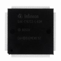
SAK-C167CS-L40M CA+ Infineon Technologies, SAK-C167CS-L40M CA+ Datasheet - Page 27

SAK-C167CS-L40M CA+
Manufacturer Part Number
SAK-C167CS-L40M CA+
Description
IC MCU 16BIT 40MHZ MQFP-144
Manufacturer
Infineon Technologies
Series
C16xxr
Datasheet
1.SAK-C167CS-LM_CA.pdf
(81 pages)
Specifications of SAK-C167CS-L40M CA+
Core Processor
C166
Core Size
16-Bit
Speed
40MHz
Connectivity
CAN, EBI/EMI, SPI, SSC, UART/USART
Peripherals
POR, PWM, WDT
Number Of I /o
111
Program Memory Type
ROMless
Ram Size
11K x 8
Voltage - Supply (vcc/vdd)
4.5 V ~ 5.5 V
Data Converters
A/D 24x10b
Oscillator Type
External
Operating Temperature
-40°C ~ 125°C
Package / Case
144- BSQFP
Data Bus Width
16 bit
Data Ram Size
11 KB
Interface Type
1xUSART, 1xSSC
Maximum Clock Frequency
40 MHz
Number Of Programmable I/os
111
Number Of Timers
9
Operating Supply Voltage
5 V
Maximum Operating Temperature
+ 125 C
Mounting Style
SMD/SMT
Minimum Operating Temperature
- 40 C
On-chip Adc
10 bit, 24 Channel
Packages
PG-MQFP-144
Max Clock Frequency
40.0 MHz
Sram (incl. Cache)
11.0 KByte
Can Nodes
2
A / D Input Lines (incl. Fadc)
24
Program Memory
0.0 KByte
Lead Free Status / RoHS Status
Lead free / RoHS Compliant
Eeprom Size
-
Program Memory Size
-
Lead Free Status / Rohs Status
Details
Other names
K167CSL40MCAZNP
K167CSL40MCAZXP
SAK-C167CS-L40M CA+
SAK-C167CS-L40MCAIN
SAKC167CSL40MCAXT
SP000103490
K167CSL40MCAZXP
SAK-C167CS-L40M CA+
SAK-C167CS-L40MCAIN
SAKC167CSL40MCAXT
SP000103490
C167CS-4R
C167CS-L
Capture/Compare (CAPCOM) Units
The CAPCOM units support generation and control of timing sequences on up to
32 channels with a maximum resolution of 16 TCL. The CAPCOM units are typically
used to handle high speed I/O tasks such as pulse and waveform generation, pulse
width modulation (PMW), Digital to Analog (D/A) conversion, software timing, or time
recording relative to external events.
Four 16-bit timers (T0/T1, T7/T8) with reload registers provide two independent time
bases for the capture/compare register array.
The input clock for the timers is programmable to several prescaled values of the internal
system clock, or may be derived from an overflow/underflow of timer T6 in module GPT2.
This provides a wide range of variation for the timer period and resolution and allows
precise adjustments to the application specific requirements. In addition, external count
inputs for CAPCOM timers T0 and T7 allow event scheduling for the capture/compare
registers relative to external events.
Both of the two capture/compare register arrays contain 16 dual purpose capture/
compare registers, each of which may be individually allocated to either CAPCOM timer
T0 or T1 (T7 or T8, respectively), and programmed for capture or compare function.
Each register has one port pin associated with it which serves as an input pin for
triggering the capture function, or as an output pin to indicate the occurrence of a
compare event.
When a capture/compare register has been selected for capture mode, the current
contents of the allocated timer will be latched (‘capture’d) into the capture/compare
register in response to an external event at the port pin which is associated with this
register. In addition, a specific interrupt request for this capture/compare register is
generated. Either a positive, a negative, or both a positive and a negative external signal
transition at the pin can be selected as the triggering event. The contents of all registers
which have been selected for one of the five compare modes are continuously compared
with the contents of the allocated timers. When a match occurs between the timer value
and the value in a capture/compare register, specific actions will be taken based on the
selected compare mode.
Data Sheet
23
V2.2, 2001-08


