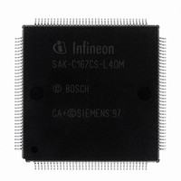
SAK-C167CS-L40M CA+ Infineon Technologies, SAK-C167CS-L40M CA+ Datasheet - Page 19

SAK-C167CS-L40M CA+
Manufacturer Part Number
SAK-C167CS-L40M CA+
Description
IC MCU 16BIT 40MHZ MQFP-144
Manufacturer
Infineon Technologies
Series
C16xxr
Datasheet
1.SAK-C167CS-LM_CA.pdf
(81 pages)
Specifications of SAK-C167CS-L40M CA+
Core Processor
C166
Core Size
16-Bit
Speed
40MHz
Connectivity
CAN, EBI/EMI, SPI, SSC, UART/USART
Peripherals
POR, PWM, WDT
Number Of I /o
111
Program Memory Type
ROMless
Ram Size
11K x 8
Voltage - Supply (vcc/vdd)
4.5 V ~ 5.5 V
Data Converters
A/D 24x10b
Oscillator Type
External
Operating Temperature
-40°C ~ 125°C
Package / Case
144- BSQFP
Data Bus Width
16 bit
Data Ram Size
11 KB
Interface Type
1xUSART, 1xSSC
Maximum Clock Frequency
40 MHz
Number Of Programmable I/os
111
Number Of Timers
9
Operating Supply Voltage
5 V
Maximum Operating Temperature
+ 125 C
Mounting Style
SMD/SMT
Minimum Operating Temperature
- 40 C
On-chip Adc
10 bit, 24 Channel
Packages
PG-MQFP-144
Max Clock Frequency
40.0 MHz
Sram (incl. Cache)
11.0 KByte
Can Nodes
2
A / D Input Lines (incl. Fadc)
24
Program Memory
0.0 KByte
Lead Free Status / RoHS Status
Lead free / RoHS Compliant
Eeprom Size
-
Program Memory Size
-
Lead Free Status / Rohs Status
Details
Other names
K167CSL40MCAZNP
K167CSL40MCAZXP
SAK-C167CS-L40M CA+
SAK-C167CS-L40MCAIN
SAKC167CSL40MCAXT
SP000103490
K167CSL40MCAZXP
SAK-C167CS-L40M CA+
SAK-C167CS-L40MCAIN
SAKC167CSL40MCAXT
SP000103490
C167CS-4R
C167CS-L
Memory Organization
The memory space of the C167CS is configured in a Von Neumann architecture which
means that code memory, data memory, registers and I/O ports are organized within the
same linear address space which includes 16 MBytes. The entire memory space can be
accessed bytewise or wordwise. Particular portions of the on-chip memory have
additionally been made directly bitaddressable.
The C167CS incorporates 32 KBytes of on-chip mask-programmable ROM (not in the
ROM-less derivative, of course) for code or constant data. The 32 KBytes of the on-chip
ROM can be mapped either to segment 0 or segment 1.
3 KBytes of on-chip Internal RAM (IRAM) are provided as a storage for user defined
variables, for the system stack, general purpose register banks and even for code. A
register bank can consist of up to 16 wordwide (R0 to R15) and/or bytewide (RL0, RH0,
…, RL7, RH7) so-called General Purpose Registers (GPRs).
1024 bytes (2 × 512 bytes) of the address space are reserved for the Special Function
Register areas (SFR space and ESFR space). SFRs are wordwide registers which are
used for controlling and monitoring functions of the different on-chip units. Unused SFR
addresses are reserved for future members of the C166 Family.
8 KBytes of on-chip Extension RAM (XRAM), organized as two blocks of 2 KByte and
6 KByte, respectively, are provided to store user data, user stacks, or code. The XRAM
is accessed like external memory and therefore cannot be used for the system stack or
for register banks and is not bitaddressable. The XRAM permits 16-bit accesses with
maximum speed.
In order to meet the needs of designs where more memory is required than is provided
on chip, up to 16 MBytes of external RAM and/or ROM can be connected to the
microcontroller.
Data Sheet
15
V2.2, 2001-08


