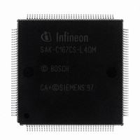
SAK-C167CS-L40M CA+ Infineon Technologies, SAK-C167CS-L40M CA+ Datasheet - Page 5

SAK-C167CS-L40M CA+
Manufacturer Part Number
SAK-C167CS-L40M CA+
Description
IC MCU 16BIT 40MHZ MQFP-144
Manufacturer
Infineon Technologies
Series
C16xxr
Datasheet
1.SAK-C167CS-LM_CA.pdf
(81 pages)
Specifications of SAK-C167CS-L40M CA+
Core Processor
C166
Core Size
16-Bit
Speed
40MHz
Connectivity
CAN, EBI/EMI, SPI, SSC, UART/USART
Peripherals
POR, PWM, WDT
Number Of I /o
111
Program Memory Type
ROMless
Ram Size
11K x 8
Voltage - Supply (vcc/vdd)
4.5 V ~ 5.5 V
Data Converters
A/D 24x10b
Oscillator Type
External
Operating Temperature
-40°C ~ 125°C
Package / Case
144- BSQFP
Data Bus Width
16 bit
Data Ram Size
11 KB
Interface Type
1xUSART, 1xSSC
Maximum Clock Frequency
40 MHz
Number Of Programmable I/os
111
Number Of Timers
9
Operating Supply Voltage
5 V
Maximum Operating Temperature
+ 125 C
Mounting Style
SMD/SMT
Minimum Operating Temperature
- 40 C
On-chip Adc
10 bit, 24 Channel
Packages
PG-MQFP-144
Max Clock Frequency
40.0 MHz
Sram (incl. Cache)
11.0 KByte
Can Nodes
2
A / D Input Lines (incl. Fadc)
24
Program Memory
0.0 KByte
Lead Free Status / RoHS Status
Lead free / RoHS Compliant
Eeprom Size
-
Program Memory Size
-
Lead Free Status / Rohs Status
Details
Other names
K167CSL40MCAZNP
K167CSL40MCAZXP
SAK-C167CS-L40M CA+
SAK-C167CS-L40MCAIN
SAKC167CSL40MCAXT
SP000103490
K167CSL40MCAZXP
SAK-C167CS-L40M CA+
SAK-C167CS-L40MCAIN
SAKC167CSL40MCAXT
SP000103490
16-Bit Single-Chip Microcontroller
C166 Family
C167CS-4R, C167CS-L
• High Performance 16-bit CPU with 4-Stage Pipeline
• 16-Priority-Level Interrupt System with 56 Sources, Sample-Rate down to 40/30/25 ns
• 8-Channel Interrupt-Driven Single-Cycle Data Transfer Facilities via
• Clock Generation via on-chip PLL (factors 1:1.5/2/2.5/3/4/5),
• On-Chip Memory Modules
• On-Chip Peripheral Modules
• Up to 16 MBytes External Address Space for Code and Data
• Idle, Sleep, and Power Down Modes with Flexible Power Management
• Programmable Watchdog Timer and Oscillator Watchdog
• Up to 111 General Purpose I/O Lines,
Data Sheet
– 80/60/50 ns Instruction Cycle Time at 25/33/40 MHz CPU Clock
– 400/303/250 ns Multiplication (16 × 16 bit), 800/606/500 ns Division (32-/16-bit)
– Enhanced Boolean Bit Manipulation Facilities
– Additional Instructions to Support HLL and Operating Systems
– Register-Based Design with Multiple Variable Register Banks
– Single-Cycle Context Switching Support
– 16 MBytes Total Linear Address Space for Code and Data
– 1024 Bytes On-Chip Special Function Register Area
Peripheral Event Controller (PEC)
via prescaler or via direct clock input
– 3 KBytes On-Chip Internal RAM (IRAM)
– 8 KBytes On-Chip Extension RAM (XRAM)
– 32 KBytes On-Chip Program Mask ROM
– 24-Channel 10-bit A/D Converter with Programmable Conversion Time
– Two 16-Channel Capture/Compare Units
– 4-Channel PWM Unit
– Two Multi-Functional General Purpose Timer Units with 5 Timers
– Two Serial Channels (Synchronous/Asynchronous and High-Speed-Synchronous)
– Two On-Chip CAN Interfaces (Rev. 2.0B active) with 2 × 15 Message Objects
– On-Chip Real Time Clock
– Programmable External Bus Characteristics for Different Address Ranges
– Multiplexed or Demultiplexed External Address/Data Buses with 8-Bit or 16-Bit
– Five Programmable Chip-Select Signals
– Hold- and Hold-Acknowledge Bus Arbitration Support
partly with Selectable Input Thresholds and Hysteresis
down to 7.8 µ s
(Full CAN/Basic CAN), can work on one bus with 30 objects
Data Bus Width
1
V2.2, 2001-08
C167CS


