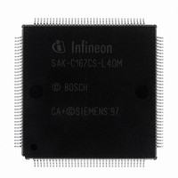
SAK-C167CS-L40M CA+ Infineon Technologies, SAK-C167CS-L40M CA+ Datasheet - Page 14

SAK-C167CS-L40M CA+
Manufacturer Part Number
SAK-C167CS-L40M CA+
Description
IC MCU 16BIT 40MHZ MQFP-144
Manufacturer
Infineon Technologies
Series
C16xxr
Datasheet
1.SAK-C167CS-LM_CA.pdf
(81 pages)
Specifications of SAK-C167CS-L40M CA+
Core Processor
C166
Core Size
16-Bit
Speed
40MHz
Connectivity
CAN, EBI/EMI, SPI, SSC, UART/USART
Peripherals
POR, PWM, WDT
Number Of I /o
111
Program Memory Type
ROMless
Ram Size
11K x 8
Voltage - Supply (vcc/vdd)
4.5 V ~ 5.5 V
Data Converters
A/D 24x10b
Oscillator Type
External
Operating Temperature
-40°C ~ 125°C
Package / Case
144- BSQFP
Data Bus Width
16 bit
Data Ram Size
11 KB
Interface Type
1xUSART, 1xSSC
Maximum Clock Frequency
40 MHz
Number Of Programmable I/os
111
Number Of Timers
9
Operating Supply Voltage
5 V
Maximum Operating Temperature
+ 125 C
Mounting Style
SMD/SMT
Minimum Operating Temperature
- 40 C
On-chip Adc
10 bit, 24 Channel
Packages
PG-MQFP-144
Max Clock Frequency
40.0 MHz
Sram (incl. Cache)
11.0 KByte
Can Nodes
2
A / D Input Lines (incl. Fadc)
24
Program Memory
0.0 KByte
Lead Free Status / RoHS Status
Lead free / RoHS Compliant
Eeprom Size
-
Program Memory Size
-
Lead Free Status / Rohs Status
Details
Other names
K167CSL40MCAZNP
K167CSL40MCAZXP
SAK-C167CS-L40M CA+
SAK-C167CS-L40MCAIN
SAKC167CSL40MCAXT
SP000103490
K167CSL40MCAZXP
SAK-C167CS-L40M CA+
SAK-C167CS-L40MCAIN
SAKC167CSL40MCAXT
SP000103490
Table 2
Symbol Pin
ALE
EA
PORT0
P0L.0-7
P0H.0-7
Data Sheet
Num.
98
99
100-
107
108,
111-
117
Pin Definitions and Functions (cont’d)
Input
Outp.
O
I
IO
Address Latch Enable Output. Can be used for latching the
Function
address into external memory or an address latch in the
multiplexed bus modes.
External Access Enable pin. A low level at this pin during and
after Reset forces the C167CS to begin instruction execution
out of external memory. A high level forces execution out of
the internal program memory.
“ROMless” versions must have this pin tied to ‘0’.
PORT0 consists of the two 8-bit bidirectional I/O ports P0L
and P0H. It is bit-wise programmable for input or output via
direction bits. For a pin configured as input, the output driver
is put into high-impedance state.
In case of an external bus configuration, PORT0 serves as
the address (A) and address/data (AD) bus in multiplexed
bus modes and as the data (D) bus in demultiplexed bus
modes.
Demultiplexed bus modes:
Data Path Width:
P0L.0 – P0L.7:
P0H.0 – P0H.7:
Multiplexed bus modes:
Data Path Width:
P0L.0 – P0L.7:
P0H.0 – P0H.7:
10
8-bit
D0 – D7
I/O
8-bit
AD0 – AD7
A8 – A15
16-bit
D0 – D7
D8 – D15
16-bit
AD0 – AD7
AD8 – AD15
C167CS-4R
V2.2, 2001-08
C167CS-L


