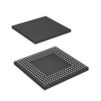
D17760BP200ADV Renesas Electronics America, D17760BP200ADV Datasheet - Page 1094

D17760BP200ADV
Manufacturer Part Number
D17760BP200ADV
Description
MPU 3V 8K,PB-FREE, 256-BGA
Manufacturer
Renesas Electronics America
Series
SuperH® SH7750r
Datasheet
1.D6417760BP200ADV.pdf
(1418 pages)
Specifications of D17760BP200ADV
Core Processor
SH-4
Core Size
32-Bit
Speed
200MHz
Connectivity
Audio Codec, CAN, EBI/EMI, FIFO, I²C, MFI, MMC, SCI, Serial Sound, SIM, SPI, USB
Peripherals
DMA, LCD, POR, WDT
Number Of I /o
69
Program Memory Type
ROMless
Ram Size
48K x 8
Voltage - Supply (vcc/vdd)
1.4 V ~ 1.6 V
Data Converters
A/D 4x10b
Oscillator Type
Internal
Operating Temperature
-40°C ~ 85°C
Package / Case
256-BGA
Lead Free Status / RoHS Status
Lead free / RoHS Compliant
Eeprom Size
-
Program Memory Size
-
Available stocks
Company
Part Number
Manufacturer
Quantity
Price
Company:
Part Number:
D17760BP200ADV
Manufacturer:
Renesas Electronics America
Quantity:
10 000
- Current page: 1094 of 1418
- Download datasheet (9Mb)
27.3.7
The MFIADR is a 32-bit register which indicates the address in the MFRAM to be accessed by the
external device via the MFI.
Specifying continuous access to the MFRAM in the LOCK bit in MFIMCR automatically
performs auto-increment (+4) or auto-decrement (-4) of the address according to the AI/AD bit in
MFIMCR, and updates MFIADR each time the external device accesses the MFRAM.
Initial value:
Initial value:
Note:
Rev. 2.00 Feb. 12, 2010 Page 1010 of 1330
REJ09B0554-0200
Bit
31 to 11
10 to 2
1, 0
R/W:
R/W:
Bit:
Bit:
* The external device can write to these bits via the MFI. The on-chip CPU cannot write to
MFI Address Register (MFIADR)
these bits.
31
15
R
R
0
0
-
-
Bit
Name
⎯
A10
to
A2
⎯
30
14
-
R
-
R
0
0
29
13
R
R
Initial
Value
All 0
All 0
All 0
0
0
-
-
28
12
R
R
0
0
-
-
R/W
R
R/W*
R
27
11
R
0
R
0
-
-
R/W*
A10
26
10
R
0
-
0
Description
Reserved
These bits are always read as 0. The write value should
always be 0.
Address
Specifies the memory space in the 2-Kbyte MFRAM to
be accessed by the external device via the MFI, with 32-
bit alignment.
Reserved
These bits are always read as 0. The write value should
always be 0.
R/W* R/W* R/W* R/W* R/W*
25
A9
R
-
0
9
0
24
A8
R
0
8
0
-
23
A7
R
0
7
0
-
22
A6
R
0
0
6
-
21
A5
R
0
0
5
-
R/W* R/W* R/W*
20
A4
R
0
4
0
-
19
A3
R
0
3
0
-
A2
18
R
0
2
0
-
17
R
0
1
-
0
R
-
16
R
0
0
R
-
0
-
Related parts for D17760BP200ADV
Image
Part Number
Description
Manufacturer
Datasheet
Request
R

Part Number:
Description:
KIT STARTER FOR M16C/29
Manufacturer:
Renesas Electronics America
Datasheet:

Part Number:
Description:
KIT STARTER FOR R8C/2D
Manufacturer:
Renesas Electronics America
Datasheet:

Part Number:
Description:
R0K33062P STARTER KIT
Manufacturer:
Renesas Electronics America
Datasheet:

Part Number:
Description:
KIT STARTER FOR R8C/23 E8A
Manufacturer:
Renesas Electronics America
Datasheet:

Part Number:
Description:
KIT STARTER FOR R8C/25
Manufacturer:
Renesas Electronics America
Datasheet:

Part Number:
Description:
KIT STARTER H8S2456 SHARPE DSPLY
Manufacturer:
Renesas Electronics America
Datasheet:

Part Number:
Description:
KIT STARTER FOR R8C38C
Manufacturer:
Renesas Electronics America
Datasheet:

Part Number:
Description:
KIT STARTER FOR R8C35C
Manufacturer:
Renesas Electronics America
Datasheet:

Part Number:
Description:
KIT STARTER FOR R8CL3AC+LCD APPS
Manufacturer:
Renesas Electronics America
Datasheet:

Part Number:
Description:
KIT STARTER FOR RX610
Manufacturer:
Renesas Electronics America
Datasheet:

Part Number:
Description:
KIT STARTER FOR R32C/118
Manufacturer:
Renesas Electronics America
Datasheet:

Part Number:
Description:
KIT DEV RSK-R8C/26-29
Manufacturer:
Renesas Electronics America
Datasheet:

Part Number:
Description:
KIT STARTER FOR SH7124
Manufacturer:
Renesas Electronics America
Datasheet:

Part Number:
Description:
KIT STARTER FOR H8SX/1622
Manufacturer:
Renesas Electronics America
Datasheet:

Part Number:
Description:
KIT DEV FOR SH7203
Manufacturer:
Renesas Electronics America
Datasheet:


