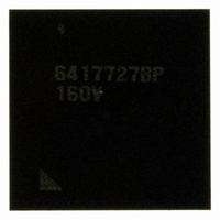
HD6417727BP160CV Renesas Electronics America, HD6417727BP160CV Datasheet - Page 756

HD6417727BP160CV
Manufacturer Part Number
HD6417727BP160CV
Description
IC SH MPU ROMLESS 240BGA
Manufacturer
Renesas Electronics America
Series
SuperH® SH7700r
Datasheet
1.HD6417727BP100CV.pdf
(1098 pages)
Specifications of HD6417727BP160CV
Core Processor
SH-3 DSP
Core Size
32-Bit
Speed
160MHz
Connectivity
FIFO, SCI, SIO, SmartCard, USB
Peripherals
DMA, LCD, POR, WDT
Number Of I /o
104
Program Memory Type
ROMless
Ram Size
32K x 8
Voltage - Supply (vcc/vdd)
1.7 V ~ 2.05 V
Data Converters
A/D 6x10b; D/A 2x8b
Oscillator Type
Internal
Operating Temperature
-20°C ~ 75°C
Package / Case
240-BGA
Package
240CSP
Family Name
SuperH
Maximum Speed
160 MHz
Operating Supply Voltage
1.8|3.3 V
Data Bus Width
32 Bit
Number Of Programmable I/os
104
Interface Type
SCI/USB
On-chip Adc
6-chx10-bit
On-chip Dac
2-chx8-bit
Number Of Timers
4
Lead Free Status / RoHS Status
Lead free / RoHS Compliant
Eeprom Size
-
Program Memory Size
-
Available stocks
Company
Part Number
Manufacturer
Quantity
Price
Company:
Part Number:
HD6417727BP160CV
Manufacturer:
LITEON
Quantity:
46 000
Company:
Part Number:
HD6417727BP160CV
Manufacturer:
Renesas Electronics America
Quantity:
10 000
- Current page: 756 of 1098
- Download datasheet (7Mb)
Section 23 USB Function Controller
23.5.9
USB Trigger Register (USBTRG)
USBTRG generates one-shot triggers to control the transmit/receive sequence for each endpoint.
Bit:
7
6
5
4
3
2
1
0
—
EP3
EP1
EP2
—
EP0s
EP0o
EP0i
PKTE
RDFN
PKTE
RDFN
RDFN
PKTE
R/W:
W
W
W
W
W
W
W
W
Bit 7—Reserved
Bit 6—EP3 Packet Enable (EP3 PKTE): After one packet of data has been written to the
endpoint 3 transmit FIFO buffer, the transmit data is fixed by writing 1 to this bit.
Bit 5—EP1 Read Complete (EP1 RDFN): Write 1 to this bit after one packet of data has been
read from the endpoint 1 FIFO buffer. The endpoint 1 receive FIFO buffer has a dual-FIFO
configuration. Writing 1 to this bit initializes the FIFO that was read, enabling the next packet to
be received.
Bit 4—Endpoint 2 Packet Enable (EP2 PKTE): After one packet of data has been written to the
endpoint 2 FIFO buffer, the transmit data is fixed by writing 1 to this bit.
Bit 3—Reserved
Bit 2—EP0s Read Complete (EP0s RDFN): Write 1 to this bit after EP0s command FIFO data
has been read. Writing 1 to this bit enables transmission/reception of data in the following data
stage. A NACK handshake is returned in response to transmit/receive requests from the host in the
data stage until 1 is written to this bit.
Bit 1—EP0o Read Complete (EP0o RDFN): Writing 1 to this bit after one packet of data has
been read from the endpoint 0 transmit FIFO buffer initializes the FIFO buffer, enabling the next
packet to be received.
Bit 0—EP0i Packet Enable (EP0i PKTE): After one packet of data has been written to the
endpoint 0 transmit FIFO buffer, the transmit data is fixed by writing 1 to this bit.
Rev.6.00 Mar. 27, 2009 Page 698 of 1036
REJ09B0254-0600
Related parts for HD6417727BP160CV
Image
Part Number
Description
Manufacturer
Datasheet
Request
R

Part Number:
Description:
KIT STARTER FOR M16C/29
Manufacturer:
Renesas Electronics America
Datasheet:

Part Number:
Description:
KIT STARTER FOR R8C/2D
Manufacturer:
Renesas Electronics America
Datasheet:

Part Number:
Description:
R0K33062P STARTER KIT
Manufacturer:
Renesas Electronics America
Datasheet:

Part Number:
Description:
KIT STARTER FOR R8C/23 E8A
Manufacturer:
Renesas Electronics America
Datasheet:

Part Number:
Description:
KIT STARTER FOR R8C/25
Manufacturer:
Renesas Electronics America
Datasheet:

Part Number:
Description:
KIT STARTER H8S2456 SHARPE DSPLY
Manufacturer:
Renesas Electronics America
Datasheet:

Part Number:
Description:
KIT STARTER FOR R8C38C
Manufacturer:
Renesas Electronics America
Datasheet:

Part Number:
Description:
KIT STARTER FOR R8C35C
Manufacturer:
Renesas Electronics America
Datasheet:

Part Number:
Description:
KIT STARTER FOR R8CL3AC+LCD APPS
Manufacturer:
Renesas Electronics America
Datasheet:

Part Number:
Description:
KIT STARTER FOR RX610
Manufacturer:
Renesas Electronics America
Datasheet:

Part Number:
Description:
KIT STARTER FOR R32C/118
Manufacturer:
Renesas Electronics America
Datasheet:

Part Number:
Description:
KIT DEV RSK-R8C/26-29
Manufacturer:
Renesas Electronics America
Datasheet:

Part Number:
Description:
KIT STARTER FOR SH7124
Manufacturer:
Renesas Electronics America
Datasheet:

Part Number:
Description:
KIT STARTER FOR H8SX/1622
Manufacturer:
Renesas Electronics America
Datasheet:

Part Number:
Description:
KIT DEV FOR SH7203
Manufacturer:
Renesas Electronics America
Datasheet:


