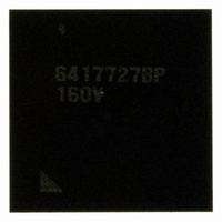
HD6417727BP160CV Renesas Electronics America, HD6417727BP160CV Datasheet - Page 696

HD6417727BP160CV
Manufacturer Part Number
HD6417727BP160CV
Description
IC SH MPU ROMLESS 240BGA
Manufacturer
Renesas Electronics America
Series
SuperH® SH7700r
Datasheet
1.HD6417727BP100CV.pdf
(1098 pages)
Specifications of HD6417727BP160CV
Core Processor
SH-3 DSP
Core Size
32-Bit
Speed
160MHz
Connectivity
FIFO, SCI, SIO, SmartCard, USB
Peripherals
DMA, LCD, POR, WDT
Number Of I /o
104
Program Memory Type
ROMless
Ram Size
32K x 8
Voltage - Supply (vcc/vdd)
1.7 V ~ 2.05 V
Data Converters
A/D 6x10b; D/A 2x8b
Oscillator Type
Internal
Operating Temperature
-20°C ~ 75°C
Package / Case
240-BGA
Package
240CSP
Family Name
SuperH
Maximum Speed
160 MHz
Operating Supply Voltage
1.8|3.3 V
Data Bus Width
32 Bit
Number Of Programmable I/os
104
Interface Type
SCI/USB
On-chip Adc
6-chx10-bit
On-chip Dac
2-chx8-bit
Number Of Timers
4
Lead Free Status / RoHS Status
Lead free / RoHS Compliant
Eeprom Size
-
Program Memory Size
-
Available stocks
Company
Part Number
Manufacturer
Quantity
Price
Company:
Part Number:
HD6417727BP160CV
Manufacturer:
LITEON
Quantity:
46 000
Company:
Part Number:
HD6417727BP160CV
Manufacturer:
Renesas Electronics America
Quantity:
10 000
- Current page: 696 of 1098
- Download datasheet (7Mb)
Section 20 Serial IO (SIOF)
(2) Control by Secondary FS
This is the method that CODEC, which outputs SIOFSYNC as a sync. pulse (FS), transmit or
receive the control data by outputting the secondary FS used for transmit or receive for only
control data after the period of 1/2 frame, which is different from the original FS output position.
Order of the control data interface as secondary FS are listed below.
• Normal data are sent as LSB=0 (compulsory is 0 by SIOF)
• Transmit data of LSB=1 at transmitting the control data
• CODEC transmits secondary FS
• SIOF synchronizes secondary FS and transmit or receive (storing into SIRCR register) the
Figure 20.8 shows timing of control data interface by secondary FS.
Rev.6.00 Mar. 27, 2009 Page 638 of 1036
REJ09B0254-0600
SCK_SIO
SIOFSYNC
TXD_SIO
RXD_SIO
(For 1 by SIOF reading to SITCR register)
control data (setting data in SITCR register)
Setting:
Slot No.0
Lch.DATA
Normal FS
TRMD = 01, REDG = 0,
TDLE = 1,
RDLE = 1,
CD0E = 1,
Figure 20.8 Control Data Interface (Secondary FS)
LSB = "1” " (secondary FS request)
1/2 frame
TDLA3 to TDLA0 = 0000,
RDLA3 to RDLA0 = 0000,
CD0A3 to CD0A0 = 0000,
1 frame
Control ch.0
Slot No.0
Secondary FS
FL = 1100 (frame length 28 bits)
TDRE = 0,
RDRE = 0,
CD1E = 0,
1/2 frame
TDRA3 to TDRA0 = 0000,
RDRA3 to RDRA0 = 0000,
CD1A3 to CD1A0 = 0000
Normal FS
Related parts for HD6417727BP160CV
Image
Part Number
Description
Manufacturer
Datasheet
Request
R

Part Number:
Description:
KIT STARTER FOR M16C/29
Manufacturer:
Renesas Electronics America
Datasheet:

Part Number:
Description:
KIT STARTER FOR R8C/2D
Manufacturer:
Renesas Electronics America
Datasheet:

Part Number:
Description:
R0K33062P STARTER KIT
Manufacturer:
Renesas Electronics America
Datasheet:

Part Number:
Description:
KIT STARTER FOR R8C/23 E8A
Manufacturer:
Renesas Electronics America
Datasheet:

Part Number:
Description:
KIT STARTER FOR R8C/25
Manufacturer:
Renesas Electronics America
Datasheet:

Part Number:
Description:
KIT STARTER H8S2456 SHARPE DSPLY
Manufacturer:
Renesas Electronics America
Datasheet:

Part Number:
Description:
KIT STARTER FOR R8C38C
Manufacturer:
Renesas Electronics America
Datasheet:

Part Number:
Description:
KIT STARTER FOR R8C35C
Manufacturer:
Renesas Electronics America
Datasheet:

Part Number:
Description:
KIT STARTER FOR R8CL3AC+LCD APPS
Manufacturer:
Renesas Electronics America
Datasheet:

Part Number:
Description:
KIT STARTER FOR RX610
Manufacturer:
Renesas Electronics America
Datasheet:

Part Number:
Description:
KIT STARTER FOR R32C/118
Manufacturer:
Renesas Electronics America
Datasheet:

Part Number:
Description:
KIT DEV RSK-R8C/26-29
Manufacturer:
Renesas Electronics America
Datasheet:

Part Number:
Description:
KIT STARTER FOR SH7124
Manufacturer:
Renesas Electronics America
Datasheet:

Part Number:
Description:
KIT STARTER FOR H8SX/1622
Manufacturer:
Renesas Electronics America
Datasheet:

Part Number:
Description:
KIT DEV FOR SH7203
Manufacturer:
Renesas Electronics America
Datasheet:


