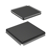
HD6417727F100C Renesas Electronics America, HD6417727F100C Datasheet - Page 87

HD6417727F100C
Manufacturer Part Number
HD6417727F100C
Description
IC SUPERH MPU ROMLESS 240QFP
Manufacturer
Renesas Electronics America
Series
SuperH® SH7700r
Datasheet
1.HD6417727BP100CV.pdf
(1098 pages)
Specifications of HD6417727F100C
Core Processor
SH-3 DSP
Core Size
32-Bit
Speed
100MHz
Connectivity
FIFO, SCI, SIO, SmartCard, USB
Peripherals
DMA, LCD, POR, WDT
Number Of I /o
104
Program Memory Type
ROMless
Ram Size
32K x 8
Voltage - Supply (vcc/vdd)
1.6 V ~ 2.05 V
Data Converters
A/D 6x10b; D/A 2x8b
Oscillator Type
Internal
Operating Temperature
-20°C ~ 75°C
Package / Case
240-QFP
Lead Free Status / RoHS Status
Contains lead / RoHS non-compliant
Eeprom Size
-
Program Memory Size
-
Available stocks
Company
Part Number
Manufacturer
Quantity
Price
Company:
Part Number:
HD6417727F100C
Manufacturer:
Renesas Electronics America
Quantity:
10 000
- Current page: 87 of 1098
- Download datasheet (7Mb)
31
MD bit:
RB bit:
BL bit:
RC [11:0]: 12-bit repeat counter
DSP bit:
DMY bit:
DMX bit:
Q, M bit:
I [3:0]:
RF [1:0]:
S bit:
T bit:
Reserved bits: Always read as 0, and should always be written with 0 (bit 31, bits 15 to 13).
0 MD
RB BL
Processor operation mode
MD = 1: Privileged mode
MD = 0: User mode
Register bank bit; used to define the general registers in privileged mode.
RB = 1:
RB = 0:
Block bit; used to mask exception in privileged mode.
BL = 1: Interrupts are masked (not accepted)
BL = 0: Interrupts are accepted
DSP operation mode
DSP = 1: DSP instructions (LDS Rm, DSR/A0/X0/X1/Y0/Y1,
DSP = 0: All DSP instructions are treated as illegal instructions; only SH3 instructions are
Modulo addressing enable for Y side
Modulo addressing enable for X side
Used by DIV0U/S and DIV1 instructions.
4-bit field indicating the interrupt request mask level.
Used for repeat control
Used by the MAC instructions and DSP data.
The MOVT, CMP/cond, TAS, TST, BT, BF, SETT, CLRT and DT instructions use the T bit to
indicate true (logic one) or false (logic zero). The ADDV/C, SUBV/C, DIV0U/S, DIV1,
NEGC, SHAR/L, SHLR/L, ROTR/L and ROTCR/L instructions also use the T bit to indicate
a carry, borrow, overflow, or underflow.
28 27
RC
16 15 13 12
R0_BANK1 to R7_BANK1 are used as general registers.
R0_BANK0 to R7_BANK0 accessed by LDC/STC instructions.
R0_BANK0 to R7_BANK0 are used as general registers.
R0_BANK1 to R7_BANK1 accessed by LDC/STC instructions.
LDS.L @Rm+, DSR/A0/X0/X1/Y0/Y1, STS DSR/A0/X0/X1/Y0/Y1, Rn,
STS.L DSR/A0/X0/X1/Y0/Y1, @−Rn, LDC Rm, RS/RE/MOD,
LDC.L @Rm+, RS/RE/MOD, STC RS/RE/MOD,Rn, STC.L RS/RE/MOD, @−Rn,
LDRS, LDRE, SETRC, MOVS, MOVX, MOVY, Pxxx) are enabled.
supported.
0-0
DSP DMY DMX M Q I3
Figure 2.5 Control Registers (1)
11
10
9
8
7
I2 I1 I0 RF1 RF0 S
6
5
Rev.6.00 Mar. 27, 2009 Page 29 of 1036
4
3
2
1
T
0
SR (Status register)
REJ09B0254-0600
Section 2 CPU
Related parts for HD6417727F100C
Image
Part Number
Description
Manufacturer
Datasheet
Request
R

Part Number:
Description:
KIT STARTER FOR M16C/29
Manufacturer:
Renesas Electronics America
Datasheet:

Part Number:
Description:
KIT STARTER FOR R8C/2D
Manufacturer:
Renesas Electronics America
Datasheet:

Part Number:
Description:
R0K33062P STARTER KIT
Manufacturer:
Renesas Electronics America
Datasheet:

Part Number:
Description:
KIT STARTER FOR R8C/23 E8A
Manufacturer:
Renesas Electronics America
Datasheet:

Part Number:
Description:
KIT STARTER FOR R8C/25
Manufacturer:
Renesas Electronics America
Datasheet:

Part Number:
Description:
KIT STARTER H8S2456 SHARPE DSPLY
Manufacturer:
Renesas Electronics America
Datasheet:

Part Number:
Description:
KIT STARTER FOR R8C38C
Manufacturer:
Renesas Electronics America
Datasheet:

Part Number:
Description:
KIT STARTER FOR R8C35C
Manufacturer:
Renesas Electronics America
Datasheet:

Part Number:
Description:
KIT STARTER FOR R8CL3AC+LCD APPS
Manufacturer:
Renesas Electronics America
Datasheet:

Part Number:
Description:
KIT STARTER FOR RX610
Manufacturer:
Renesas Electronics America
Datasheet:

Part Number:
Description:
KIT STARTER FOR R32C/118
Manufacturer:
Renesas Electronics America
Datasheet:

Part Number:
Description:
KIT DEV RSK-R8C/26-29
Manufacturer:
Renesas Electronics America
Datasheet:

Part Number:
Description:
KIT STARTER FOR SH7124
Manufacturer:
Renesas Electronics America
Datasheet:

Part Number:
Description:
KIT STARTER FOR H8SX/1622
Manufacturer:
Renesas Electronics America
Datasheet:

Part Number:
Description:
KIT DEV FOR SH7203
Manufacturer:
Renesas Electronics America
Datasheet:


