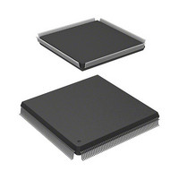
HD6417727F100C Renesas Electronics America, HD6417727F100C Datasheet - Page 220

HD6417727F100C
Manufacturer Part Number
HD6417727F100C
Description
IC SUPERH MPU ROMLESS 240QFP
Manufacturer
Renesas Electronics America
Series
SuperH® SH7700r
Datasheet
1.HD6417727BP100CV.pdf
(1098 pages)
Specifications of HD6417727F100C
Core Processor
SH-3 DSP
Core Size
32-Bit
Speed
100MHz
Connectivity
FIFO, SCI, SIO, SmartCard, USB
Peripherals
DMA, LCD, POR, WDT
Number Of I /o
104
Program Memory Type
ROMless
Ram Size
32K x 8
Voltage - Supply (vcc/vdd)
1.6 V ~ 2.05 V
Data Converters
A/D 6x10b; D/A 2x8b
Oscillator Type
Internal
Operating Temperature
-20°C ~ 75°C
Package / Case
240-QFP
Lead Free Status / RoHS Status
Contains lead / RoHS non-compliant
Eeprom Size
-
Program Memory Size
-
Available stocks
Company
Part Number
Manufacturer
Quantity
Price
Company:
Part Number:
HD6417727F100C
Manufacturer:
Renesas Electronics America
Quantity:
10 000
- Current page: 220 of 1098
- Download datasheet (7Mb)
Section 6 X/Y Memory
6.2
The X/Y memory can be located in either map-enabled area or fixed-mapped area, depending on
the mode bit (MD) and DSP bit (DSP) setting in the status register (SR). Figure 6.1 shows X/Y
memory logical mapping.
1. Privileged Mode
2. User Mode
3. Privileged-DSP Mode
4. User-DSP Mode
It is recommended that for the mappable area, the C (cacheable) bit in the TLB entry must be set
to 0 to guarantee a two-cycle access.
Mapping through TLB translation provides a flexible X/Y memory addressing scheme but takes
two cycles even when the C bit in the TLB entry is cleared to 0. Fixed mapping provides a one-
cycle access for read and two-cycle access for write, which is the appropriate method for mission-
critical realtime operations.
Rev.6.00 Mar. 27, 2009 Page 162 of 1036
REJ09B0254-0600
MD = 1, DSP = 0; Any physical address in space P0 or P3 can map to X/Y memory through
TLB translation. Addresses ranging from H'A500 0000 to H'A5FF FFFF in the P2 space can
also fixed map to X/Y memory. Since the DSP extension is disabled, the DSP instruction set
and registers are not available to the programmer.
MD = 0, DSP = 0; Any physical address in the U0 space can access X/Y memory through TLB
translation. Any access to addresses beyond the U0 space will cause an address error. Since the
DSP extension is disabled, the DSP instruction set and registers are not available to the
programmer.
MD = 1, DSP = 1; Any physical address in space P0 or P3 can map to X/Y memory through
TLB translation. Addresses ranging from H'A500 0000 to H'A5FF FFFF in the P2 space can
also fixed-map to X/Y memory. Since the DSP extension is enabled, the DSP instruction set
and registers are available to the programmer.
MD = 0, DSP = 1; Any physical address in space U0 can map to X/Y memory through TLB
translation. Addresses ranging from H'A500 0000 to H'A5FF FFFF in the Uxy spaces can also
fixed map to X/Y memory. Any access to outside of U0 and Uxy space will cause an address
error. Since the DSP extension is enabled, the DSP instruction set and registers are available to
the programmer.
X/Y Memory Access from the CPU
Related parts for HD6417727F100C
Image
Part Number
Description
Manufacturer
Datasheet
Request
R

Part Number:
Description:
KIT STARTER FOR M16C/29
Manufacturer:
Renesas Electronics America
Datasheet:

Part Number:
Description:
KIT STARTER FOR R8C/2D
Manufacturer:
Renesas Electronics America
Datasheet:

Part Number:
Description:
R0K33062P STARTER KIT
Manufacturer:
Renesas Electronics America
Datasheet:

Part Number:
Description:
KIT STARTER FOR R8C/23 E8A
Manufacturer:
Renesas Electronics America
Datasheet:

Part Number:
Description:
KIT STARTER FOR R8C/25
Manufacturer:
Renesas Electronics America
Datasheet:

Part Number:
Description:
KIT STARTER H8S2456 SHARPE DSPLY
Manufacturer:
Renesas Electronics America
Datasheet:

Part Number:
Description:
KIT STARTER FOR R8C38C
Manufacturer:
Renesas Electronics America
Datasheet:

Part Number:
Description:
KIT STARTER FOR R8C35C
Manufacturer:
Renesas Electronics America
Datasheet:

Part Number:
Description:
KIT STARTER FOR R8CL3AC+LCD APPS
Manufacturer:
Renesas Electronics America
Datasheet:

Part Number:
Description:
KIT STARTER FOR RX610
Manufacturer:
Renesas Electronics America
Datasheet:

Part Number:
Description:
KIT STARTER FOR R32C/118
Manufacturer:
Renesas Electronics America
Datasheet:

Part Number:
Description:
KIT DEV RSK-R8C/26-29
Manufacturer:
Renesas Electronics America
Datasheet:

Part Number:
Description:
KIT STARTER FOR SH7124
Manufacturer:
Renesas Electronics America
Datasheet:

Part Number:
Description:
KIT STARTER FOR H8SX/1622
Manufacturer:
Renesas Electronics America
Datasheet:

Part Number:
Description:
KIT DEV FOR SH7203
Manufacturer:
Renesas Electronics America
Datasheet:


