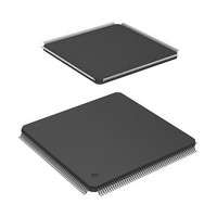
HD6417705F133BV Renesas Electronics America, HD6417705F133BV Datasheet - Page 80

HD6417705F133BV
Manufacturer Part Number
HD6417705F133BV
Description
MPU 3V 0K PB-FREE 208 FP
Manufacturer
Renesas Electronics America
Series
SuperH® SH7700r
Datasheet
1.HD6417705F133BV.pdf
(741 pages)
Specifications of HD6417705F133BV
Core Processor
SH-3
Core Size
32-Bit
Speed
133MHz
Connectivity
EBI/EMI, FIFO, IrDA, SCI, USB
Peripherals
DMA, POR, PWM, WDT
Number Of I /o
105
Program Memory Type
ROMless
Ram Size
32K x 8
Voltage - Supply (vcc/vdd)
1.4 V ~ 1.6 V
Data Converters
A/D 4x10b
Oscillator Type
Internal
Operating Temperature
-20°C ~ 75°C
Package / Case
208-LQFP
Lead Free Status / RoHS Status
Lead free / RoHS Compliant
Eeprom Size
-
Program Memory Size
-
- Current page: 80 of 741
- Download datasheet (5Mb)
2.3.1
General Registers
There are twenty-four 32-bit general registers: R0_BANK0 to R7_BANK0, R0_BANK1 to
R7_BANK1, and R8 to R15. R0 to R7 are banked. The process mode and the register bank (RB)
bit in the status register (SR) define which set of banked registers (R0_BANK0 to R7_BANK0 or
R0_BANK1 to R7_BANK1) are accessed as general registers. R0 to R7 registers in the selected
bank are accessed as R0 to R7. R0 to R7 in the non-selected bank is accessed as R0_BANK to
R7_BANK by the control register load instruction (LDC) and control register store instruction
(STC).
In user mode, bank 0 is selected regardless of he RB bit value. Sixteen registers: R0_BANK0 to
R7_BANK0 and R8 to R15 are accessed as general registers R0 to R15. The R0_BANK1 to
R7_BANK1 registers in bank 1 cannot be accessed.
In privileged mode that is entered by a transition to exception handling state, the RB bit is set to 1
to select bank 1. In privileged mode, sixteen registers: R0_BANK1 to R7_BANK1 and R8 to R15
are accessed as general registers R0 to R15. A bank is switched automatically when an exception
handling state is entered, registers R0 to R7 need not be saved by the exception handling routine.
The R0_BANK0 to R7_BANK0 registers in bank 0 can be accessed as R0_BANK to R7_BANK
by the LDC and STC instructions.
In privileged mode, bank 0 can also be used as general registers by clearing the RB bit to 0. In this
case, sixteen registers: R0_BANK0 to R7_BANK0 and R8 to R15 are accessed as general
registers R0 to R15. The R0_BANK1 to R7_BANK1 registers in bank 1 can be accessed as
R0_BANK to R7_BANK by the LDC and STC instructions.
The general registers R0 to R15 are used as equivalent registers for almost all instructions. In
some instructions, the R0 register is automatically used or only the R0 register can be used as
source or destination registers.
Rev. 2.00, 09/03, page 32 of 690
Related parts for HD6417705F133BV
Image
Part Number
Description
Manufacturer
Datasheet
Request
R

Part Number:
Description:
KIT STARTER FOR M16C/29
Manufacturer:
Renesas Electronics America
Datasheet:

Part Number:
Description:
KIT STARTER FOR R8C/2D
Manufacturer:
Renesas Electronics America
Datasheet:

Part Number:
Description:
R0K33062P STARTER KIT
Manufacturer:
Renesas Electronics America
Datasheet:

Part Number:
Description:
KIT STARTER FOR R8C/23 E8A
Manufacturer:
Renesas Electronics America
Datasheet:

Part Number:
Description:
KIT STARTER FOR R8C/25
Manufacturer:
Renesas Electronics America
Datasheet:

Part Number:
Description:
KIT STARTER H8S2456 SHARPE DSPLY
Manufacturer:
Renesas Electronics America
Datasheet:

Part Number:
Description:
KIT STARTER FOR R8C38C
Manufacturer:
Renesas Electronics America
Datasheet:

Part Number:
Description:
KIT STARTER FOR R8C35C
Manufacturer:
Renesas Electronics America
Datasheet:

Part Number:
Description:
KIT STARTER FOR R8CL3AC+LCD APPS
Manufacturer:
Renesas Electronics America
Datasheet:

Part Number:
Description:
KIT STARTER FOR RX610
Manufacturer:
Renesas Electronics America
Datasheet:

Part Number:
Description:
KIT STARTER FOR R32C/118
Manufacturer:
Renesas Electronics America
Datasheet:

Part Number:
Description:
KIT DEV RSK-R8C/26-29
Manufacturer:
Renesas Electronics America
Datasheet:

Part Number:
Description:
KIT STARTER FOR SH7124
Manufacturer:
Renesas Electronics America
Datasheet:

Part Number:
Description:
KIT STARTER FOR H8SX/1622
Manufacturer:
Renesas Electronics America
Datasheet:

Part Number:
Description:
KIT DEV FOR SH7203
Manufacturer:
Renesas Electronics America
Datasheet:


