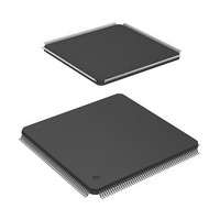
HD6417705F133BV Renesas Electronics America, HD6417705F133BV Datasheet - Page 604

HD6417705F133BV
Manufacturer Part Number
HD6417705F133BV
Description
MPU 3V 0K PB-FREE 208 FP
Manufacturer
Renesas Electronics America
Series
SuperH® SH7700r
Datasheet
1.HD6417705F133BV.pdf
(741 pages)
Specifications of HD6417705F133BV
Core Processor
SH-3
Core Size
32-Bit
Speed
133MHz
Connectivity
EBI/EMI, FIFO, IrDA, SCI, USB
Peripherals
DMA, POR, PWM, WDT
Number Of I /o
105
Program Memory Type
ROMless
Ram Size
32K x 8
Voltage - Supply (vcc/vdd)
1.4 V ~ 1.6 V
Data Converters
A/D 4x10b
Oscillator Type
Internal
Operating Temperature
-20°C ~ 75°C
Package / Case
208-LQFP
Lead Free Status / RoHS Status
Lead free / RoHS Compliant
Eeprom Size
-
Program Memory Size
-
- Current page: 604 of 741
- Download datasheet (5Mb)
5. When selecting the I bus as the break condition, note the following:
6. While the block bit (BL) in the CPU status register (SR) is set to 1, no breaks can be accepted.
Rev. 2.00, 09/03, page 556 of 690
However, condition determination will be carried out, and if the condition matches, the
corresponding condition match flag is set to 1.
Several bus masters, including the CPU and DMAC, are connected to the I bus. The UBC
monitors bus cycles generated by all bus masters, and determines the condition match.
Physical addresses are used for the I bus. Set a physical address in break address registers
(BARA and BARB). The bus cycles for logical addresses issued on the L bus by the CPU
are converted to physical addresses before being output to the I bus. (If the address
translation function is enabled, address translation by the MMU is carried out.)
For data access cycles issued on the L bus by the CPU, if their logical addresses are not to
be cached, they are issued with the data size specified on the L bus and their addresses are
not rounded.
For instruction fetch cycles issued on the L bus by the CPU, even though their logical
addresses are not to be cached, they are issued in longwords and their addresses are
rounded to match longword boundaries.
If a logical address issued on the L bus by the CPU is an address to be cached and a cache
miss occurs, its bus cycle is issued as a cache fill cycle on the I bus. In this case, it is issued
in longwords and its address is rounded to match longword boundaries. However note that
cache fill is not performed for a write miss in write through mode. In this case, the bus
cycle is issued with the data size specified on the L bus and its address is not rounded. In
write back mode, a write back cycle may be issued in addition to a read fill cycle. It is a
longword bus cycle whose address is rounded to match longword boundaries.
I bus cycles (including read fill cycles) resulting from instruction fetches on the L bus by
the CPU are defined as instruction fetch cycles on the I bus, while other bus cycles are
defined as data access cycles.
The DMAC only issues data access cycles for I bus cycles.
If a break condition is specified for the I bus, even when the condition matches in an I bus
cycle resulting from an instruction executed by the CPU, at which instruction the break is
to be accepted cannot be clearly defined.
Related parts for HD6417705F133BV
Image
Part Number
Description
Manufacturer
Datasheet
Request
R

Part Number:
Description:
KIT STARTER FOR M16C/29
Manufacturer:
Renesas Electronics America
Datasheet:

Part Number:
Description:
KIT STARTER FOR R8C/2D
Manufacturer:
Renesas Electronics America
Datasheet:

Part Number:
Description:
R0K33062P STARTER KIT
Manufacturer:
Renesas Electronics America
Datasheet:

Part Number:
Description:
KIT STARTER FOR R8C/23 E8A
Manufacturer:
Renesas Electronics America
Datasheet:

Part Number:
Description:
KIT STARTER FOR R8C/25
Manufacturer:
Renesas Electronics America
Datasheet:

Part Number:
Description:
KIT STARTER H8S2456 SHARPE DSPLY
Manufacturer:
Renesas Electronics America
Datasheet:

Part Number:
Description:
KIT STARTER FOR R8C38C
Manufacturer:
Renesas Electronics America
Datasheet:

Part Number:
Description:
KIT STARTER FOR R8C35C
Manufacturer:
Renesas Electronics America
Datasheet:

Part Number:
Description:
KIT STARTER FOR R8CL3AC+LCD APPS
Manufacturer:
Renesas Electronics America
Datasheet:

Part Number:
Description:
KIT STARTER FOR RX610
Manufacturer:
Renesas Electronics America
Datasheet:

Part Number:
Description:
KIT STARTER FOR R32C/118
Manufacturer:
Renesas Electronics America
Datasheet:

Part Number:
Description:
KIT DEV RSK-R8C/26-29
Manufacturer:
Renesas Electronics America
Datasheet:

Part Number:
Description:
KIT STARTER FOR SH7124
Manufacturer:
Renesas Electronics America
Datasheet:

Part Number:
Description:
KIT STARTER FOR H8SX/1622
Manufacturer:
Renesas Electronics America
Datasheet:

Part Number:
Description:
KIT DEV FOR SH7203
Manufacturer:
Renesas Electronics America
Datasheet:


