DF2367VF33V Renesas Electronics America, DF2367VF33V Datasheet - Page 624
DF2367VF33V
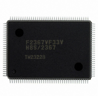
Manufacturer Part Number
DF2367VF33V
Description
IC H8S/2367 MCU FLASH 128QFP
Manufacturer
Renesas Electronics America
Series
H8® H8S/2300r
Datasheets
1.HEWH8E10A.pdf
(19 pages)
2.D12312SVTE25V.pdf
(341 pages)
3.DF2368VTE34V.pdf
(1044 pages)
Specifications of DF2367VF33V
Core Processor
H8S/2000
Core Size
16-Bit
Speed
33MHz
Connectivity
I²C, IrDA, SCI, SmartCard
Peripherals
DMA, POR, PWM, WDT
Number Of I /o
84
Program Memory Size
384KB (384K x 8)
Program Memory Type
FLASH
Ram Size
24K x 8
Voltage - Supply (vcc/vdd)
3 V ~ 3.6 V
Data Converters
A/D 10x10b, D/A 2x8b
Oscillator Type
Internal
Operating Temperature
-20°C ~ 75°C
Package / Case
128-QFP
For Use With
YR0K42378FC000BA - KIT EVAL FOR H8S/2378HS0005KCU11H - EMULATOR E10A-USB H8S(X),SH2(A)
Lead Free Status / RoHS Status
Lead free / RoHS Compliant
Eeprom Size
-
Available stocks
Company
Part Number
Manufacturer
Quantity
Price
Company:

Part Number:
DF2367VF33V
Manufacturer:
Renesas Electronics America
Quantity:
135
Company:
Part Number:
DF2367VF33V
Manufacturer:
Renesas Electronics America
Quantity:
10 000


Section 14 Serial Communication Interface (SCI, IrDA)
14.3.9
BRR is an 8-bit register that adjusts the bit rate. As the SCI performs baud rate generator control
independently for each channel, different bit rates can be set for each channel. Table 14.2 shows
the relationships between the N setting in BRR and bit rate B for normal asynchronous mode,
clocked synchronous mode, and Smart Card interface mode. The initial value of BRR is H'FF, and
it can be read or written to by the CPU at all times.
Table 14.2 Relationships between N Setting in BRR and Bit Rate B
Notes: B: Bit rate (bit/s)
Table 14.3 shows sample N settings in BRR in normal asynchronous mode. Table 14.4 shows the
maximum bit rate for each frequency in normal asynchronous mode. Table 14.6 shows sample N
settings in BRR in clocked synchronous mode. Table 14.8 shows sample N settings in BRR in
Smart Card interface mode. In Smart Card interface mode, S (the number of basic clock periods in
a 1-bit transfer interval) can be selected. For details, refer to section 14.7.4, Receive Data
Sampling Timing and Reception Margin. Tables 14.5 and 14.7 show the maximum bit rates with
external clock input.
Rev.6.00 Mar. 18, 2009 Page 564 of 980
REJ09B0050-0600
Mode
Asynchronous
Mode
Clocked
Synchronous
Mode
Smart Card
Interface Mode
CKS1
0
0
1
1
N: BRR setting for baud rate generator (0 ≤ N ≤ 255)
φ: Operating frequency (MHz)
n and S: Determined by the SMR settings shown in the following tables.
SMR Setting
Bit Rate Register (BRR)
CKS0
0
1
0
1
Bit Rate
B =
B =
B =
64
S
8
2
2
2
2n-1
2n-1
2n-1
n
0
1
2
3
10
10
10
(N + 1)
(N + 1)
6
6
6
(N + 1)
Error
Error (%) = {
Error (%) = {
BCP1
0
0
1
1
SMR Setting
B
B
64
S
BCP0
0
1
0
1
2
2
2n-1
2n-1
10
10
6
6
(N + 1)
(N + 1)
S
32
64
372
256
- 1 }
- 1 }
100
100
Related parts for DF2367VF33V
Image
Part Number
Description
Manufacturer
Datasheet
Request
R

Part Number:
Description:
CONN PLUG 12POS DUAL 0.5MM SMD
Manufacturer:
Hirose Electric Co Ltd
Datasheet:
Part Number:
Description:
CONN PLUG 18POS DUAL 0.5MM SMD
Manufacturer:
Hirose Electric Co Ltd
Datasheet:
Part Number:
Description:
CONN PLUG 14POS DUAL 0.5MM SMD
Manufacturer:
Hirose Electric Co Ltd
Datasheet:
Part Number:
Description:
CONN RECEPT 20POS DUAL 0.5MM SMD
Manufacturer:
Hirose Electric Co Ltd
Datasheet:
Part Number:
Description:
CONN PLUG 16POS DUAL 0.5MM SMD
Manufacturer:
Hirose Electric Co Ltd
Datasheet:
Part Number:
Description:
CONN RECEPT 16POS DUAL 0.5MM SMD
Manufacturer:
Hirose Electric Co Ltd
Datasheet:
Part Number:
Description:
CONN PLUG 20POS DUAL 0.5MM SMD
Manufacturer:
Hirose Electric Co Ltd
Datasheet:
Part Number:
Description:
CONN PLUG 30POS DUAL 0.5MM SMD
Manufacturer:
Hirose Electric Co Ltd
Datasheet:
Part Number:
Description:
CONN RECEPT 30POS DUAL 0.5MM SMD
Manufacturer:
Hirose Electric Co Ltd
Datasheet:
Part Number:
Description:
CONN PLUG 40POS DUAL 0.5MM SMD
Manufacturer:
Hirose Electric Co Ltd
Datasheet:

Part Number:
Description:
KIT STARTER FOR M16C/29
Manufacturer:
Renesas Electronics America
Datasheet:

Part Number:
Description:
KIT STARTER FOR R8C/2D
Manufacturer:
Renesas Electronics America
Datasheet:

Part Number:
Description:
R0K33062P STARTER KIT
Manufacturer:
Renesas Electronics America
Datasheet:

Part Number:
Description:
KIT STARTER FOR R8C/23 E8A
Manufacturer:
Renesas Electronics America
Datasheet:

Part Number:
Description:
KIT STARTER FOR R8C/25
Manufacturer:
Renesas Electronics America
Datasheet: