DF2367VF33V Renesas Electronics America, DF2367VF33V Datasheet - Page 38
DF2367VF33V
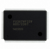
Manufacturer Part Number
DF2367VF33V
Description
IC H8S/2367 MCU FLASH 128QFP
Manufacturer
Renesas Electronics America
Series
H8® H8S/2300r
Datasheets
1.HEWH8E10A.pdf
(19 pages)
2.D12312SVTE25V.pdf
(341 pages)
3.DF2368VTE34V.pdf
(1044 pages)
Specifications of DF2367VF33V
Core Processor
H8S/2000
Core Size
16-Bit
Speed
33MHz
Connectivity
I²C, IrDA, SCI, SmartCard
Peripherals
DMA, POR, PWM, WDT
Number Of I /o
84
Program Memory Size
384KB (384K x 8)
Program Memory Type
FLASH
Ram Size
24K x 8
Voltage - Supply (vcc/vdd)
3 V ~ 3.6 V
Data Converters
A/D 10x10b, D/A 2x8b
Oscillator Type
Internal
Operating Temperature
-20°C ~ 75°C
Package / Case
128-QFP
For Use With
YR0K42378FC000BA - KIT EVAL FOR H8S/2378HS0005KCU11H - EMULATOR E10A-USB H8S(X),SH2(A)
Lead Free Status / RoHS Status
Lead free / RoHS Compliant
Eeprom Size
-
Available stocks
Company
Part Number
Manufacturer
Quantity
Price
Company:

Part Number:
DF2367VF33V
Manufacturer:
Renesas Electronics America
Quantity:
135
Company:
Part Number:
DF2367VF33V
Manufacturer:
Renesas Electronics America
Quantity:
10 000


20.4 On-Board Programming Mode ......................................................................................... 748
20.5 Protection .......................................................................................................................... 778
20.6 Switching between User MAT and User Boot MAT ........................................................ 781
20.7 Programmer Mode ............................................................................................................ 782
20.8 Serial Communication Interface Specification for Boot Mode......................................... 782
20.9 Usage Notes ...................................................................................................................... 810
Section 21 Mask ROM
Section 22 Clock Pulse Generator
22.1 Register Descriptions ........................................................................................................ 813
22.2 Oscillator........................................................................................................................... 816
22.3 PLL Circuit ....................................................................................................................... 818
22.4 Frequency Divider ............................................................................................................ 819
22.5 Usage Notes ...................................................................................................................... 819
Section 23 Power-Down Modes
23.1 Register Descriptions ........................................................................................................ 826
23.2 Operation .......................................................................................................................... 830
Rev.6.00 Mar. 18, 2009 Page xxxvi of lviii
REJ09B0050-0600
20.3.2 Programming/Erasing Interface Parameter .......................................................... 735
20.3.3 Flash Vector Address Control Register (FVACR)............................................... 747
20.4.1 Boot Mode ........................................................................................................... 748
20.4.2 User Program Mode............................................................................................. 753
20.4.3 User Boot Mode................................................................................................... 764
20.4.4 Procedure Program and Storable Area for Programming Data ............................ 768
20.5.1 Hardware Protection ............................................................................................ 778
20.5.2 Software Protection.............................................................................................. 779
20.5.3 Error Protection.................................................................................................... 779
22.1.1 System Clock Control Register (SCKCR) ........................................................... 814
22.1.2 PLL Control Register (PLLCR)........................................................................... 815
22.2.1 Connecting a Crystal Oscillator ........................................................................... 816
22.2.2 External Clock Input ............................................................................................ 817
22.5.1 Notes on Clock Pulse Generator .......................................................................... 819
22.5.2 Notes on Oscillator .............................................................................................. 820
22.5.3 Notes on Board Design ........................................................................................ 820
23.1.1 Standby Control Register (SBYCR) .................................................................... 826
23.1.2 Module Stop Control Registers H and L (MSTPCRH, MSTPCRL).................... 828
23.1.3 Extension Module Stop Control Registers H and L
23.2.1 Clock Division Mode........................................................................................... 830
(EXMSTPCRH, EXMSTPCRL) ......................................................................... 829
....................................................................................................... 811
...................................................................................... 823
.................................................................................. 813
Related parts for DF2367VF33V
Image
Part Number
Description
Manufacturer
Datasheet
Request
R

Part Number:
Description:
CONN PLUG 12POS DUAL 0.5MM SMD
Manufacturer:
Hirose Electric Co Ltd
Datasheet:
Part Number:
Description:
CONN PLUG 18POS DUAL 0.5MM SMD
Manufacturer:
Hirose Electric Co Ltd
Datasheet:
Part Number:
Description:
CONN PLUG 14POS DUAL 0.5MM SMD
Manufacturer:
Hirose Electric Co Ltd
Datasheet:
Part Number:
Description:
CONN RECEPT 20POS DUAL 0.5MM SMD
Manufacturer:
Hirose Electric Co Ltd
Datasheet:
Part Number:
Description:
CONN PLUG 16POS DUAL 0.5MM SMD
Manufacturer:
Hirose Electric Co Ltd
Datasheet:
Part Number:
Description:
CONN RECEPT 16POS DUAL 0.5MM SMD
Manufacturer:
Hirose Electric Co Ltd
Datasheet:
Part Number:
Description:
CONN PLUG 20POS DUAL 0.5MM SMD
Manufacturer:
Hirose Electric Co Ltd
Datasheet:
Part Number:
Description:
CONN PLUG 30POS DUAL 0.5MM SMD
Manufacturer:
Hirose Electric Co Ltd
Datasheet:
Part Number:
Description:
CONN RECEPT 30POS DUAL 0.5MM SMD
Manufacturer:
Hirose Electric Co Ltd
Datasheet:
Part Number:
Description:
CONN PLUG 40POS DUAL 0.5MM SMD
Manufacturer:
Hirose Electric Co Ltd
Datasheet:

Part Number:
Description:
KIT STARTER FOR M16C/29
Manufacturer:
Renesas Electronics America
Datasheet:

Part Number:
Description:
KIT STARTER FOR R8C/2D
Manufacturer:
Renesas Electronics America
Datasheet:

Part Number:
Description:
R0K33062P STARTER KIT
Manufacturer:
Renesas Electronics America
Datasheet:

Part Number:
Description:
KIT STARTER FOR R8C/23 E8A
Manufacturer:
Renesas Electronics America
Datasheet:

Part Number:
Description:
KIT STARTER FOR R8C/25
Manufacturer:
Renesas Electronics America
Datasheet: