DF2367VF33V Renesas Electronics America, DF2367VF33V Datasheet - Page 195
DF2367VF33V
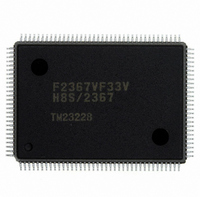
Manufacturer Part Number
DF2367VF33V
Description
IC H8S/2367 MCU FLASH 128QFP
Manufacturer
Renesas Electronics America
Series
H8® H8S/2300r
Datasheets
1.HEWH8E10A.pdf
(19 pages)
2.D12312SVTE25V.pdf
(341 pages)
3.DF2368VTE34V.pdf
(1044 pages)
Specifications of DF2367VF33V
Core Processor
H8S/2000
Core Size
16-Bit
Speed
33MHz
Connectivity
I²C, IrDA, SCI, SmartCard
Peripherals
DMA, POR, PWM, WDT
Number Of I /o
84
Program Memory Size
384KB (384K x 8)
Program Memory Type
FLASH
Ram Size
24K x 8
Voltage - Supply (vcc/vdd)
3 V ~ 3.6 V
Data Converters
A/D 10x10b, D/A 2x8b
Oscillator Type
Internal
Operating Temperature
-20°C ~ 75°C
Package / Case
128-QFP
For Use With
YR0K42378FC000BA - KIT EVAL FOR H8S/2378HS0005KCU11H - EMULATOR E10A-USB H8S(X),SH2(A)
Lead Free Status / RoHS Status
Lead free / RoHS Compliant
Eeprom Size
-
Available stocks
Company
Part Number
Manufacturer
Quantity
Price
Company:

Part Number:
DF2367VF33V
Manufacturer:
Renesas Electronics America
Quantity:
135
Company:
Part Number:
DF2367VF33V
Manufacturer:
Renesas Electronics America
Quantity:
10 000


6.3.8
DRAMCR is used to make DRAM/synchronous DRAM interface settings.
Bit
15
14
13
12
11
Bit Name
OEE
RAST
−
CAST
−
DRAM Control Register (DRAMCR)
Initial Value
0
0
0
0
0
R/W
R/W
R/W
R/W
R/W
R/W
Description
OE Output Enable
The OE signal used when EDO page mode
DRAM is connected can be output from the
(OE) pin. The OE signal is common to all
areas designated as DRAM space.
0: OE signal output disabled
1: OE signal output enabled
RAS Assertion Timing Select
Selects whether, in DRAM access, the RAS
signal is asserted from the start of the T
(rising edge of φ) or from the falling edge of φ.
Figure 6.4 shows the relationship between the
RAST bit setting and the RAS assertion timing.
The setting of this bit applies to all areas
designated as DRAM space.
0: RAS is asserted from φ falling edge in T
1: RAS is asserted from start of T
Reserved
Though this bit can be read from or written to,
the write value should always be 0.
Column Address Output Cycle Number Select
Selects whether the column address output
cycle in DRAM access comprises 3 states or 2
states. The setting of this bit applies to all
areas designated as DRAM space.
0: 2-state column address output cycle
1: 3-state column address output cycle
Reserved
Though this bit can be read from or written to,
the write value should always be 0.
(OE) pin can be used as I/O port
cycle
Rev.6.00 Mar. 18, 2009 Page 135 of 980
Section 6 Bus Controller (BSC)
REJ09B0050-0600
r
cycle
r
cycle
r
Related parts for DF2367VF33V
Image
Part Number
Description
Manufacturer
Datasheet
Request
R

Part Number:
Description:
CONN PLUG 12POS DUAL 0.5MM SMD
Manufacturer:
Hirose Electric Co Ltd
Datasheet:
Part Number:
Description:
CONN PLUG 18POS DUAL 0.5MM SMD
Manufacturer:
Hirose Electric Co Ltd
Datasheet:
Part Number:
Description:
CONN PLUG 14POS DUAL 0.5MM SMD
Manufacturer:
Hirose Electric Co Ltd
Datasheet:
Part Number:
Description:
CONN RECEPT 20POS DUAL 0.5MM SMD
Manufacturer:
Hirose Electric Co Ltd
Datasheet:
Part Number:
Description:
CONN PLUG 16POS DUAL 0.5MM SMD
Manufacturer:
Hirose Electric Co Ltd
Datasheet:
Part Number:
Description:
CONN RECEPT 16POS DUAL 0.5MM SMD
Manufacturer:
Hirose Electric Co Ltd
Datasheet:
Part Number:
Description:
CONN PLUG 20POS DUAL 0.5MM SMD
Manufacturer:
Hirose Electric Co Ltd
Datasheet:
Part Number:
Description:
CONN PLUG 30POS DUAL 0.5MM SMD
Manufacturer:
Hirose Electric Co Ltd
Datasheet:
Part Number:
Description:
CONN RECEPT 30POS DUAL 0.5MM SMD
Manufacturer:
Hirose Electric Co Ltd
Datasheet:
Part Number:
Description:
CONN PLUG 40POS DUAL 0.5MM SMD
Manufacturer:
Hirose Electric Co Ltd
Datasheet:

Part Number:
Description:
KIT STARTER FOR M16C/29
Manufacturer:
Renesas Electronics America
Datasheet:

Part Number:
Description:
KIT STARTER FOR R8C/2D
Manufacturer:
Renesas Electronics America
Datasheet:

Part Number:
Description:
R0K33062P STARTER KIT
Manufacturer:
Renesas Electronics America
Datasheet:

Part Number:
Description:
KIT STARTER FOR R8C/23 E8A
Manufacturer:
Renesas Electronics America
Datasheet:

Part Number:
Description:
KIT STARTER FOR R8C/25
Manufacturer:
Renesas Electronics America
Datasheet: